Download
1 / 52
550 likes | 710 Views
Introduction to Programmable Logic Devices. John Coughlan STFC Technology Department Detector & Electronics Division. PPD Lectures. Programmable Logic is a Key Underlying Technology for PP Experiments. First-Level and High-Level Triggering Data Transport (Networks)

E N D
Introduction toProgrammable Logic Devices John Coughlan STFC Technology Department Detector & Electronics Division
PPD Lectures Programmable Logic is a Key Underlying Technology for PP Experiments. • First-Level and High-Level Triggering • DataTransport (Networks) • Computers interacting with Hardware (Networks) • Silicon Trackers (Millions of Data Channels) Commercial Devices. Developments driven by Industry. Telecomms, Gaming, Aerospace, Automotive, Set-top boxes….
Particle Physics Electronics CMS Custom Electronics Chips ASICs ANALOGUE $$$ Rad Hard, Low Power CERN LHC
Particle Physics Electronics CMS Custom Electronics Chips ASICs ANALOGUE $$$ Rad Hard, Low Power CERN LHC Electronics Rooms Trigger Systems. DAQ Systems. DIGITAL Custom Digital Processing Boards VMEBus Crates
Particle Physics Electronics • Special Dedicated Logic Functions (not possible in CPUs) • Ultra Fast Trigger Systems (Trigger Algorithms) Clock Accurate Timing • Massively Parallel Data Processing (Silicon Trackers with Millions of Channels) Custom Designed Printed Circuit Boards PCBs. Commercial Programmable Logic Devices, FPGAs
CMS DAQ/Trigger Architectures CMS Fully custom PP ASICs Programmable Logic DIGITAL CPUs Commodity PCs “Telecoms Network” ~ 1 Tbps
Lecture Outline • Programmable Logic Devices • Basics • Evolution • FPGA Field Programmable Gate Array • Architecture • Design Flow • Hardware Description Languages • Design Tools
Digital Logic Logic Gates
Digital Logic Logic Gates Transistor Switches
Digital Logic Logic Gates MOORE’S LAW Transistor Switches < 40 nm ! $$$
Digital Logic Function Product AND (&) Sum OR (|) 3 Inputs SUM of PRODUCTS Black Box Truth Table (Look Up Table LUT) Digital Logic
Digital Logic Function Product AND (&) Sum OR (|) 3 Inputs SUM of PRODUCTS Black Box Truth Table (Look Up Table LUT) Digital Logic
Digital Logic Function Product AND (&) Sum OR (|) 3 Inputs SUM of PRODUCTS Black Box Truth Table (Look Up Table LUT) Digital Logic
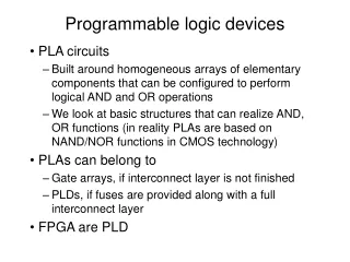
Programmable Logic Devices PLDs Inputs • SUM of PRODUCTS • (Re-)Programmble Links • Reconfigurable • GLUE LOGIC Un-programmed State ANDs Planes of ANDs, ORs ORs Outputs Logic Functions
Programmable Logic Devices PLDs Inputs • SUM of PRODUCTS • (Re-)Programmble Links • Reconfigurable • GLUE LOGIC Un-programmed State ANDs Planes of ANDs, ORs ORs Outputs Logic Functions
Programmable Logic Devices PLDs Inputs • SUM of PRODUCTS • (Re-)Programmble Links • Reconfigurable • GLUE LOGIC Un-programmed State ANDs Planes of ANDs, ORs ORs Outputs Logic Functions
Programmable Logic Devices PLDs Inputs • SUM of PRODUCTS • (Re-)Programmble Links • Reconfigurable • GLUE LOGIC Un-programmed State ANDs Planes of ANDs, ORs ORs Outputs Logic Functions Sums Programmed PLD Product Terms
Programmable Logic Devices PLDs Logic Functions Programmed PLD Sums Product Terms
Programmable Logic Devices PLDs Logic Functions x x x Programmed PLD x x Sums Product Terms
Programmable Logic Devices PLDs • GLUE LOGIC Logic Functions x x x x Programmed PLD x x x Sums Product Terms
CPLD Architecture Complex PLDs • CPLDs • Programmable PLD Blocks • Programmable Interconnects • Electrically Erasable links Feedback Outputs
Sequential Circuits • Combinational Logic (Larger circuits difficult to predict) • Synchronous Logic driven by a CLOCK • Registers, Flip Flops (Memory) Inputs
Sequential Circuits • Combinational Logic (Larger circuits difficult to predict) • Synchronous Logic driven by a CLOCK • Registers, Flip Flops (Memory) Intermediate New Output every clock edge Inputs Register CLOCK EDGES
Sequential Circuits • Combinational Logic (Larger circuits difficult to predict) • Synchronous Logic driven by a CLOCK • Registers, Flip Flops (Memory) Intermediate New Output every clock edge Inputs Clock Rate determines speed Comb Logic Must meet Timing => Predictable circuits Register CLOCK Shift Registers, Pipelines, Finite State Machines … EDGES
Field Programmable Gate Arrays FPGA • FieldProgrammable Gate Array • ‘Simple’ Programmable Logic Blocks • Massive Fabric of Programmable Interconnects • Standard CMOS Integrated Circuit fabrication processas for memory chips (Moore’s Law)
Field Programmable Gate Arrays FPGA • FieldProgrammable Gate Array • ‘Simple’ Programmable Logic Blocks • Massive Fabric of Programmable Interconnects • Standard CMOS Integrated Circuit fabrication processas for SRAM memory chips (Moore’s Law) Huge Density of Logic Block ‘Islands’ 1,000 … 100,000’s in a ‘Sea’ of Interconnects FPGA Architecture
Logic Blocks • Logic Functions implemented in Look Up Table LUTs. • Flip-Flops. Registers. Clocked Storage elements. • Multiplexers (select 1 of N inputs) FPGA Fabric Logic Block
Look Up Tables LUTs • LUT contains Memory Cells to implement small logic functions • Each cell holds ‘0’ or ‘1’ . • Programmed with outputs of Truth Table • Inputs select content of one of the cells as output 3 Inputs LUT -> 8 Memory Cells 3 – 6 Inputs Static Random Access Memory SRAM cells Multiplexer MUX
Look Up Tables LUTs • LUT contains Memory Cells to implement small logic functions • Each cell holds ‘0’ or ‘1’ . • Programmed with outputs of Truth Table • Inputs select content of one of the cells as output • Configured by re-programmable SRAM memory cells 3 Inputs LUT -> 8 Memory Cells 3 – 6 Inputs Static Random Access Memory SRAM cells Multiplexer MUX
Logic Blocks • Larger Logic Functions built up by connecting many Logic Blocks together
Logic Blocks • Larger Logic Functions built up by connecting many Logic Blocks together • Determined by SRAM cells SRAM cells
Clocked Logic • Registers on outputs. CLOCKED storage elements. • Synchronous FPGA Logic Design, Pipelined Logic. • FPGA Fabric Pulse from Global Clock (e.g. LHC BX frequency) FPGA Fabric Special Routing for Clocks Clock from Outside world (eg LHC bunch frequency)
Input Output I/O Getting data in and out Up to > 1,000 I/O “pins” (several 100 MHz)
Input Output I/O Getting data in and out Up to > 1,000 I/O “pins” (several 100 MHz) Special I/O SERIALISERS ~ 10 Gbps transfer rates Optical TRx
Designing Logic with FPGAs • Design Capture. • High level Description of Logic Design. • Graphical descriptions • Hardware Description Language (Textual)
Hardware Description Languages • Language describing hardware (Engineers call it FIRMWARE) • Doesn’t behave like “normal” programming language ‘C/C++’ • Describe Logic as collection of Processes operating in Parallel • Language Constructs for Synchronous Logic • Compiler (Synthesis) Tools recognise certain code constructs and generates appropriate logic • Not all constructs can be implemented in FPGA! • 2 Popular languages are VHDL , VERILOG • Easy to start learning… Hard to master!
VHDL ENTITY Declaration Input Output to Module (STD LOGIC) SIGNALS Declaration WIRES CONCURRENT ASSIGNMENTS CONDITIONAL ASSIGNMENTS => MULTIPLEXERS
VHDL PROCESS Declaration. CONCURRENT functions. Synchronous Logic. COMPONENT Declaration
Designing Logic with FPGAs • High level Description of Logic Design • Hardware Description Language (Textual) • Compile (Synthesis) into NETLIST. • Boolean Logic Gates. • Target FPGA Device • Mapping • Routing • Bit File for FPGA • Commercial CAE Tools (Complex & Expensive) • Logic Simulation Design Flow
Designing Logic with FPGAs • High level Description of Logic Design • Hardware Description Language (Textual) • Compile (Synthesis) into NETLIST. • Boolean Logic Gates. • Target FPGA Device • Mapping • Routing • Bit File for FPGA • Commercial CAE Tools (Complex & Expensive) • Logic Simulation Design Flow
Designing Logic with FPGAs • High level Description of Logic Design • Hardware Description Language (Textual) • Compile (Synthesis) into NETLIST. • Boolean Logic Gates. • Target FPGA Device • Mapping • Routing • Bit File for FPGA • Commercial CAE Tools (Complex & Expensive) • Logic Simulation Design Flow
Configuring an FPGA • Millions of SRAMcells holding LUTs and Interconnect Routing • Volatile Memory. Lose configuration when board power is turned off. • Keep Bit Pattern describing the SRAM cells in non-Volatile Memory e.g. PROM or Digital Camera card • Configuration takes ~ secs JTAG Port
Configuring an FPGA • Millions of SRAMcells holding LUTs and Interconnect Routing • Volatile Memory. Lose configuration when board power is turned off. • Keep Bit Pattern describing the SRAM cells in non-Volatile Memory e.g. PROM or Digital Camera card • Configuration takes ~ secs JTAG Port Programming Bit File JTAG Testing
Field Programmable Gate Arrays FPGA • Large Complex Functions • Re-Programmability, Flexibility. • Massively Parallel Architecture • Processing many channels simultaneously cf MicroProcessor • Fast Turnaround Designs • Standard IC Manufacturing Processes. Moore’s Law • Mass produced. Inexpensive. • Many variants. Sizes. Features. • PP Not Radiation Hard • Power Hungry • No Analogue
FPGA Trends • State of Art is 40nm on 300 mm wafers • Top of range >500,000 Logic Blocks • >1,000 pins (Fine Pitched BGA) • Logic Block cost ~ 1$ in 1990 • Today < 0.1 cent • Problems • Power. Leakage currents. • Design Gap • CAE Tools
Summary • Programmable Logic Devices • Basics • Evolution • FPGA Field Programmable Gate Arrays • Architecture • Design Flow • Hardware Description Languages • Design Tools Importance for Particle Physics Experiments
References • The Design Warrior’s Guide to FPGAs • Clive Maxfield, Newnes Elsevier • VHDL for Logic Synthesis • Andrew Rushden, Wiley • FPGA manufacturer web sites • www.xilinx.com • www.altera.com • FPGA Online • www.pldesignline.com • www.fpgajournal.com • www.doulos.com
System on a Chip • Add Embedded Micro-Processor Cores in Fabric • e.g. RISC PowerPC • Ethernet Interface • Run Operating System e.g. Linux • Combine Micro-Processor & Massively Parallel Logic • Dual Design Flows • Firmware HDL • Software C