Download
1 / 12
120 likes | 210 Views
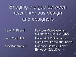
Bridging the gap between asynchronous design and designers. Peter A. Beerel Fulcrum Microsystems, Calabasas Hills, CA, USA Jordi Cortadella Universitat Polit è cnica de Catalunya, Barcelona, Spain Alex Kondratyev Cadence Berkeley Labs, Berkeley, CA, USA. R. CL. R. CL. R. CL.

E N D
Bridging the gap between asynchronous designand designers Peter A. Beerel Fulcrum Microsystems, Calabasas Hills, CA, USA Jordi Cortadella Universitat Politècnica de Catalunya, Barcelona, Spain Alex Kondratyev Cadence Berkeley Labs, Berkeley, CA, USA
R CL R CL R CL R CLK Synchronous circuit Implicit (global) synchronization between blocks Clock period > Max Delay (CL + R)
Asynchronous circuit Ack R CL R CL R CL R Req Explicit (local) synchronization: Req / Ack handshakes
Globally Async Locally Sync (GALS) Asynchronous World Clocked Domain Req3 Req1 R R CL Ack3 Ack1 Local CLK Req4 Req2 Ack4 Ack2 Async-to-sync Wrapper
Synchronous communication • Clock edges determine the time instants where data must be sampled • Data wires may glitch between clock edges(set–up/hold times must be satisfied) • Data are transmitted at a fixed rate(clock frequency) 1 1 0 0 1 0
Dual rail 1 1 1 • Two wires with L(low) and H (high) per bit • “LL” = “spacer”, “LH” = “0”, “HL” = “1” • n–bit data communication requires 2n wires • Each bit is self-timed • Other delay-insensitive codes exist (e.g. k-of-n)and event–based signalling (choice criteria: pin and power efficiency) 0 0 0
Bundled data • Validity signal • Similar to an aperiodic local clock • n–bit data communication requires n+1 wires • Data wires may glitch when no valid • Signaling protocols • level sensitive (latch) • transition sensitive (register): 2–phase / 4–phase 1 1 0 0 1 0
Asynchronous modules DATA PATH • Signaling protocol: reqin+ start+ [computation] done+ reqout+ ackout+ ackin+reqin- start- [reset] done- reqout- ackout- ackin-(more concurrency is also possible) Data IN Data OUT start done req in req out CONTROL ack in ack out
Vdd A B Z B A Gnd C-element: Other implementations Vdd A Weak inverter B Z B A Dynamic Quasi-Static Gnd
done C Completion detection tree Completion detection Dual-rail logic • • • • • •
start done delay Bundled-data logic blocks Single-rail logic • • • • • • Conventional logic + matched delay
C C C delay delay delay Micropipelines (Sutherland 89) Aout Ain C L logic L logic L logic L Rin Rout