Download
1 / 39
490 likes | 822 Views
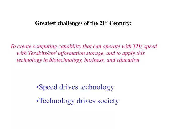
Greatest challenges of the 21 st Century:. To create computing capability that can operate with THz speed with Terabits/cm 2 information storage, and to apply this technology in biotechnology, business, and education. Speed drives technology Technology drives society.

E N D
Greatest challenges of the 21st Century: To create computing capability that can operate with THz speed with Terabits/cm2 information storage, and to apply this technology in biotechnology, business, and education • Speed drives technology • Technology drives society
“Terascale electronics---endless quest for IC speed” Toh-Ming Lu lut@rpi.edu; www.rpi.edu/~lut Director Center for Advanced Interconnect Science and Technology (RPI, SUNY-Albany, MIT, UT-Austin, N. Texas, Texas Tech., Cornell, UC Berkeley, Columbia, Georgia Tech, Rochester, U. of Maryland) Outline End of scaling Systems technologies: on-chip/off-chip interconnect Nanoelectronics
Information age? Execution, storage, and transmission of massive information What technology drives the information age? Hardware in Computer: Chips, hard drives, display……. -----Microelectronics technology
Technology for Information age--------Microelectronics • Electronics industry: driving force of the information age. largest manufacturing industry in the United States and in the developed world • Over ~14% per year growth in the last 30 years --- continue to grow in the next few decades • Will need a continuing supply of BS, MS, and Ph.D
Who are chip makers? Intel, IBM, Motorola, AMD, DEC, LSI Logic, National Semiconductor, Lucent, TI, HP….. DELL, Compaq, Gateway…don’t make chips!
History • Invention of solid state electronics (40’s) --------The transistors • Then IC • Then Mainframe (60’s)----execution and storage • Then PC (70’s)----execution and storage • Then PC plus internet plus WWW -----execution, storage, and transmission
Why so exciting? • Intellectually stimulating • Impact: changes the society in major way • Business: creates enormous wealth • Education: fundamentally change the way we learn • Medicine:will change the way we treat diseases
“Turmoil and opportunities at the dawn of the 21st Century ---the road of an academic department in higher education” (Toh-Ming Lu, amazon.com, 2000)
Computer logic---a series of on and off operation (clicks) • Imaging a super fast telegraph! (1GHz: 1000 million clicks per second; 1THz = 1000GHz) • “Fast” means: more clicks per second • The narrower the “click” the faster you get • The shorter the device the narrower the click time
Key questions in the industry Technical: ---Is there an end to increase IC speed? Business: ---Is there a market for super fast ICs?
Some key technological challenges ---Limit on device dimension ---Limit on interconnect speed
Recent news: • Intel: 1 THz FET, 25nm channel length • IBM: 210 GHz HBT, base 100 atoms
Limits on patterning: diffraction resist metal
Limit on RC delay Chip cross section
Interconnect (RC) delay Through wires time time To avoid overlapping Reduce the number of “clicks” per second ---separate the “clicks” apart Therefore reduce the speed
“Terascale electronics---endless quest for IC speed” Toh-Ming Lu lut@rpi.edu; www.rpi.edu/~lut Director Center for Advanced Interconnect Science and Technology (RPI, SUNY-Albany, MIT, UT-Austin, N. Texas, Texas Tech., Cornell, UC Berkeley, Columbia, Georgia Tech, Rochester, U. of Maryland) Outline End of scaling Systems technologies: on-chip/off-chip interconnect Nanoelectronics
3D heterogeneous systems: bonding, alignment, via etching/filling High bandwidth: to optoelectronics systems (THz) ? GaAs/Si? --killer tech A/D, sensors, IP cores Mitsubishi Electronics America: ADVANCED PACKAGINGJune/July 2000 issue. memory Logic layers PC, communications, internect… I/O, passives, power Heat extractors --Shorter wires, higher density, more functionalility— Beyond Roadmap
Opportunities for more Si mainstream technologies: ---Decades beyond the Roadmap • Stacked chip assemblies (logic, memories, interposer for passives); • Heterogeneous systems for sensors and MEMS; • Hard IP core-based SOC designs (including mixed signal); • High speed processors; • LAN architectures (for wireless applications and/or for multiplexed interconnects). Gutmann et al (2001)
J. Lu et al Pictorial Representation of 3D Integration Conceptusing Wafer Bonding, * Figure adapted from IBM Corporation and used with permission.
Processing issues: • bonding-alignment • through wafer via etching • barrier and metallization • Reliability: • thermo and mechanical stability • electromigration • heat extraction
Broad band interconnect technology • ---high speed data transfer • Replacing electrical connection by optics: • Modulators/switches: electro-optic, optic-optic • Optical waveguides • Data compression (software) Or:wireless! switches Modulators guide light fiber Chip stack
Nonlinear EO Modulated light light Electrical signal Electro-optic modulator R. Kersting, G. Stasser, and K. Unterrainer, Terahertz phase modulator, Electr. Lett., 36, 1156 (2000)
Optical switches: • MEMS---mirror switches: D. Bishop et al, Physics Today Oct 2001 (Lucent) • Nanotube switches: Zao et al (2001)---THz speed • Quantum dots switches: Dutta et al (2001)---THz speed MEMS
Potentially viable optical interconnect schemes—Dr. Persans waveguide CMOS circuits and metallization optoelectronic transceivers • Bump-bond optoelectronic chip on top of complete CMOS package • Grow optoelectronic components monolithically; local microphotonic waveguides grown and patterned; polymer waveguide layers for off-chip and longer distance • Monolithic optoelectronic components; incorporate longer waveguides into metal interconnect package • Use waveguides within sensor-chip or system-on-a-chip paradigm metal or multilayer dielectric mirror cladding waveguide via receiver Agarwal, Ponoth, Plawsky, Persans: Appl. Phys. Lett. 78, 2294 (2001)
Mainstream computer/communication technology: • Strong industrial/State/Federal partner support • Enormous employment opportunities • Decades of growth---expected more growth in decades • End of device scaling does not • imply end of Si technologies!
Emerging technologies • Nano-scale electronics: very rich and unexplored science • Strong Government support • Long term benefits (not likely mainstream computing • in at least 20 years) • ---The greatest and immediate impact may not be in electronics, • but in biomedical applications
“Terascale electronics---endless quest for IC speed” Toh-Ming Lu lut@rpi.edu; www.rpi.edu/~lut Director Center for Advanced Interconnect Science and Technology (RPI, SUNY-Albany, MIT, UT-Austin, N. Texas, Texas Tech., Cornell, UC Berkeley, Columbia, Georgia Tech, Rochester, U. of Maryland) Outline End of scaling Systems technologies: on-chip/off-chip interconnect Nanoelectronics
Deep sub-0.1 U g 2D Gate Gate electron Insulator fl u id Drain Source Plasma wave Interconnects via Terahertz Receiver-transmitter pairs • ULSI chip divided in tiles • Communicate via plasma wave electronics receiver-transmitter pairs Michael S. Shur http://nina.ecse.rpi.edu/shur/
Room temperature single electron transistor using nanotube Smalley group (2001)
Oriented & interconnected nanotube networks—Ajayan et al Focused Ions • Local modification and Junction formation • Termination (cutting of structures)
Fantastic opportunities in applied and basic science research • Examples: • New materials synthesis: polymers; nitrides, carbides • Novel polymer-metal, polymer-cermic, polymer-polymer composites: • Novel phase separation, crystallization, dynamic growth phenomena • Novel interfacial diffusion, reactions, and transformations • Novel nano-structure science; light emitting nano semiconductors • Novel non-linear thin film materials; high electro-optic coefficient materials • Novel opto-electronics materials, layered structures • Quantum effect on narrow lines • Materials response under extreme speed and frequency • Real time atomic scale microscopies
THzBio-Chip for Sensitive Detection Nano-Si or nano-C layer glass plate reference chip sample chip THz grating helps coupling THz wave THz signature or fingerprint of genetic materials: DNA, RNA or Protein attach to nano-layer in sample chip, from 10 GHz to 10 THz frequency range. (Zhang, Kersting)
Yesterday On-Chip Interconnect Today 3-Dimensional Interconnect “Norton” Facility (IC Laboratory) Tomorrow 3D Chips • Microsystems • Non-Electronic Chips • Scalable Systems 5”-8” 2µ CMOS MCR (Wafer Processing R&D) Terascale electronics? Bio-devices? 8” State-of-the-Art Wafer Fab • Welcome students doing PhD at Rensselaer • Welcome visiting scholars and collaboration
Electrical Storages • Memory:Trenches/Stacked capacitors • Passives capacitors
Magnetic storage • ---towards terabits/in2 • C. Ross, Annu. Rev. Mater. • Res. 2001. 31:203-235. • Three strategies: • exchange-decoupled grains • (conventional) • In-plane patterned media • Perpendicular patterned media
Limits on magnetization: ---Nayak/Wang/Korniss (Physics) P ? H P H
Molecular memories: Materials Today (Feb 2002)