Download
1 / 28
280 likes | 485 Views
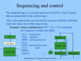
n. n-1. 10111 multiplicant 10011 multiplier 00000 initial partial prod. 10111 010111 partial product after 10111 shift 1000101 1000101. multiplicant. PC. Register A. log 2 n. Zero detect. Parallel Addr. Z. Q 0. C out. Go. Control unit. multiplier.

E N D
n n-1 10111 multiplicant 10011 multiplier 00000 initial partial prod. 10111 010111 partial product after 10111 shift 1000101 1000101 multiplicant PC Register A log2n Zero detect Parallel Addr Z Q0 Cout Go Control unit multiplier 0 C Sh Register A Sh Register Q 4 Q0 Sequencing and control The datapath logic is activated and inactivated by control signals that are generated by the control logic. Also, microoperations are executed in sequence and the controller must also take care of that sequencing. Example: binary multiplication437 = 23 19 is executed in a sequence of adds and shifts. Digital Design Ed F. Deprettere Leiden University
Recall: digital systems can be programmable or nonprogrammable. Programmable: Instructions are used and a program is a sequece of instructions usually stored in memory. Where to take operands, what operation to execute, where to put result… Nonprogrammable First A Program Counter (PC) is needed to enumerate the instructions and to change the ordering of the instructions depending on the status bits (conditional control). Executing an instruction means activating the sequence of Ops required to perform the operation specified by the instruction. Nonprogrammable: No instructions, so no instruction sequencing and no PC. Control unit determines operations to be performed and the order of the operations from inputs and status only. In bothe cases, the control unit can be hardwired or microprogrammed. this is a matter of implementation. In contrast to an instruction program, a microprogram is not visible to user Digital Design Ed F. Deprettere Leiden University
ASM resembles conventional flowchart (sequence of procedural steps and decision paths) but is closer to hardware: sequence of events + timing relationships between states of control unit and datapath actions occurring in the states in response to clock pulses. Sequence state machine A data-processing task can be defined by register transfer operations controlled by a sequencing machine specified by A (hardware) algorithm that is a sort of high level state diagram called (Algorithmic) state machine chart. Digital Design Ed F. Deprettere Leiden University
Entry Entry IDLE 000 State Binary Register Operation or Output R <- 0 RUN Exit Exit Chart Symbols State box(state in control sequence) Register Operation or Output activated while control unit in the state. Activation of an output signal means assigning a value of 1 to the signal. Example: state symbolic name is IDLE and code of 000. Inside is a register transfer operation R <- 0 (reset to zero on any clock pulse while control in state IDLE) and an output RUN (output signal RUN is 1 during time that control is in state IDLE). RUN is 1 for any state box in which it appears and 0 for any state box in which it does not appear. Digital Design Ed F. Deprettere Leiden University
Entry Entry Exit0 n-bit Condition 1-bit condition 0 1 n Exit 2 -1 Exit 0 Exit 1 Entry Register operation or output Exit Chart Symbols (cont’d) Decision box (scalar or vector) Condition is single binary input variable or Boolean expression depending only on inputs. Conditional output box Entry to conditional output box from a state box must pass through one or more decision boxes. If conditions specified on path from state box to conditional output box are satisfied, then register operations or outputs are activated. Digital Design Ed F. Deprettere Leiden University
Entry IDLE ASM BLOCK AVAIL Exit Go 0 1 A 0 0 Q0 1 Exit Exit MUL0 MUL1 Back to Binary Multiplier ASM block One state box and all decision and conditional output boxes connected between state box exit and entry paths to the same or other state boxes. While in state IDLE, output AVAIL is ‘1’ .If Go is zero, then back to IDLE, otherwise, at clock event, A is cleared, and next state is either MUL0 or MUL1 depending on Q0. ASM chart is really a form of state diagram for a sequential circuit part of the control unit. Digital Design Ed F. Deprettere Leiden University
Timing positive edge trigger cycle 1 cycle 2 cycle 3 clock go Q0 state IDLE MUL1 AVAIL 0023 0000 A Timing Positive edge-triggered flip-flops. Clock cycle 1: state is IDLE, output AVAIL is 1, and input GO is 0. When clock goes high, IDLE, AVAIL and A don’t change. Input GO goes high. Only at next clock pulse change state, output signal and register content: IDLE goes to MUL1, AVAIL goes to 0 (because it is not an output of MUL1!) and A gets cleared. Digital Design Ed F. Deprettere Leiden University
IDLE n multiplicant Register B 0 1 Go Parallel Addr Note: Value of P (Z) is checked before P is decremented! This is because Z is performed asynchronously and Register Transfer operation is synchronous with next positive clock edge. Thus: Decision on P preceeeds update of P. C 0, A 0 P n-1 Cout multiplier MUL0 0 C Register A Register Q Q0 n-1 0 1 Q0 PC A A + B, C Cout log2n Zero detect Z Q0 MUL1 Go Control unit C 0, C||A||Q sr C||A||Q, P P-1 4 0 1 Z Multiplier ASM Chart. Start when Go is 1. From state IDLE to MUL0: C and A cleared and P loaded with n-1. Decision is made: if Q0 1 then A <- A+B and carry out to C, else no change. In state MUL1: C <- 0, A(n-1) <- C, A <- srA, Q(n-1) <- A(0), Q <- sr Q. Notation (composite) C <- 0, C||A||Q <- sr C||A||Q P is decremented as well. Digital Design Ed F. Deprettere Leiden University
Module Microoperation Control Signal Name Control Expression Register A A <- 0 Initialize IDLE.G A <- A+B Load MUL0.Q C||A||Q <- sr C||A||Q Shift_Dec MUL1 Register B B <- IN Load_B LOADB Flip-Flop C C <- 0 Clear_C IDLE.G + MUL1 C <- CoutLoad MUL0.Q Register Q Q <- IN Load_Q LOADQ C||A||Q <- sr C||A||Q Shift_Dec MUL1 Counter P P <- n-1 Initialize IDLE0.G P <- P-1 Shift_Dec MUL1 Hardware Control From ASM, derive • Control Signal Table (corresponding to output parts of sequential circuit) • Next-state-behavior modified ASM (corresponding to next-state parts of • sequential circuit). Control Signals Table (Multiplier) Digital Design Ed F. Deprettere Leiden University
IDLE 00 0 1 G MUL0 01 MUL1 10 0 1 Z Hardware Control (cont’d) Sequencing part of ASM (modified ASM) chart. Remove from ASM information on microoperations leaving sequencing information. Digital Design Ed F. Deprettere Leiden University
M0 clear_C Go D Z DECODER IDLE A0 0 1 2 3 MUL0 MUL1 A1 shift_dec M1 D load STATE TABLE Q0 Current Next State Inputs State Decoder Out Name M1 M0 Go Z M1 M0 IDLE MUL0 MUL1 clock IDLE 0 0 0 x 0 0 1 0 0 0 0 1 x 0 1 1 0 0 MUL0 0 1 x x 1 0 0 1 0 MUL1 1 0 x 0 0 1 0 0 1 1 0 x 1 0 0 0 0 1 ------ 1 1 x x x x x x x Design 1: Sequence Register and Decoder iniit Digital Design Ed F. Deprettere Leiden University
Entry IDLE ASM BLOCK AVAIL entry exit entry State D Exit Go C 0 1 entry exit X A 0 A0 EN entry X DEMUX 0 Q0 1 Exit Exit D0 D1 exit_1 exit_0 MUL0 MUL1 exit_0 exit_1 entry X entry entry_1 entry_2 e_1 e_2 X exit exit exit exit Design 2: 1 FF per state Digital Design Ed F. Deprettere Leiden University
IDLE IDLE Go D 0 1 Go C 0, A 0 P n-1 init MUL0 clear_C Q0 MUL0 load D 0 1 Q0 A A + B, C Cout MUL1 shift_dec D Z MUL1 C 0, C||A||Q sr C||A||Q, P P-1 Clock 0 1 Z Complete binary multiplier. Digital Design Ed F. Deprettere Leiden University
Control inputs Status signals from datapath Next-address generator sequencer Control address register Control address Address ROM Memory Data next-address info Control data regist Microinstruction Control signals to datapath Control outputs Microprogrammed Control Digital Design Ed F. Deprettere Leiden University
9 8 6 5 4 3 0 • NEXTADD1 NEXTADD0 SEL DATAP IDLE Microinstruction control word 0 1 Go INIT C 0, A 0 P n-1 Corresponding Register Transfers A 0, P n-1 A A+B, C Cout C 0 C||A||Q sr C||A||Q MUL0 0 1 Q0 ADD A A + B, C Cout MUL1 C 0, C||A||Q sr C||A||Q, P P-1 0 1 Z There are four control signals Initialize, Load, Clear_C, Shift_dec Corresponding states INIT, ADD, INIT/MUL1, MUL0 Microinstruction bit positions 0, 1, 2, 3 Symbolic Notation (control) IT, LD, CC, SD Remaining part of control word is for the sequencing Digital Design Ed F. Deprettere Leiden University
Control inputs IDLE Status signals from datapath Next-address generator sequencer 0 1 Go Control address register INIT C 0, A 0 P n-1 Control address MUL0 Address ROM Memory Data Control data regist 0 1 Microinstruction Q0 ADD Next address info Control signals to datapath A A + B, C Cout Control outputs MUL1 5 states 5 codewords 5 addresses C 0, C||A||Q sr C||A||Q, P P-1 4+3+3+2 control signals 12 bits/word select next addresses 0 1 Z datapath Digital Design Ed F. Deprettere Leiden University
Address Symbolic transfer IDLE G: CAR INIT, G:CAR IDLE INIT C 0, A 0, P n-1, CAR MUL0 MUL0 Q0: CAR ADD, Q0: CAR MUL1 ADD A A+B, C Cout,, CAR MUL1 MUL1 C 0, C||A||Q sr C||A||Q, Z: CAR IDLE, Z: CAR MUL0, P P-1 IDLE 0 1 Go INIT C 0, A 0 P n-1 MUL0 0 1 Q0 ADD A A + B, C Cout MUL1 C 0, C||A||Q sr C||A||Q, P P-1 0 1 Z Digital Design Ed F. Deprettere Leiden University
n Datapath 2 4 n 2-to-1 MUX DATAP SEL NXTADD0 NEXTADD1 CAR 512 Control Mem (ROM) 3 3 0 1 4-to-1 MUX s 0 Go Q0 Z 0 1 2 3 3 3 Symbolic and BinaryMicroprogram S1 S0 2 Address NEXTADD1 NEXTADD0 SELL DATAPATH IDLE INIT IDLE DG None 000 001 000 01 0000 INIT ------ MULO NXT IT, CC 001 000 010 00 0101 MULO ADD MUL1 DQ None ADD ------- MUL1 NXT LD MUL1 IDLE MUL0 DZ CC, SR Digital Design Ed F. Deprettere Leiden University
n data input lines k address lines RAM 2k words Read Write n bits per word n data output lines Random Access Memories Recall: registers are small, yet fast place holders with elementary operations. When going one step up in the memory hierarchy, we find: Example: Read-only memory (ROM) Random Access Memory (RAM) k = 10 is 1K words N = 16 = 2 bytes: 2K byte RAM Time to get in (write) a word and time to get out (read) a word is independent of the location (address) of the word in memory. Word is a number of bytes. Digital Design Ed F. Deprettere Leiden University
memory content first byte second byte memoryaddress binarydecimal 0000000000 0 0000000001 1 0000000010 2 1111111101 1021 1111111110 1022 1111111111 1023 The operations: Write: store data from … into RAM - apply binary address of location to address lines -apply data bits of word to bestored to data input lines - active R/W signal (R/W = 0) Read: load data from RAM into … - apply binary address of word to read to address lines - activate R/W signal(R/W = 1) Current RAMs are real big. For Multimedia applications, they are way too small. Digital Design Ed F. Deprettere Leiden University
Types of RAMs Static Ram (SRAM) : latches are basic storage units. Dynamic Ram (DRAM) : capacitors (charge reservoirs) are the basic storage units. SRAM: larger, higher power consumption, faster DRAM: smaller, lower power consumption, slower DRAM needs refreshing because capacitors leak. Both types are volatile : power off is loss of data. Write to disc before power switch-off (disc is non-volatile) Digital Design Ed F. Deprettere Leiden University
Select B C S R C • B Select = 0 : (S = R =0) : hold Q; C = C = 0. Select = 1: S = B, C = Q Building SRAMs A RAM of m words of n bits consists of an array of n m binary storage cells plus circuitry. A RAM cell is typically designed as an electronic circuit not a logic circuit. (a matter of efficiency). But it can be modeled as a logic circuit (not so for DRAM). Digital Design Ed F. Deprettere Leiden University
Address lines A3 3 2 1 0 4-to-16 DECODER 2 2 2 2 word select A2 0 1 2 3 14 15 RAM cell 4 A1 16 * 1 RAM Dout A0 D in R/W RAM cell EN Dout Data Out Din Data In R/W Read/Write RAM select Bit Select The RAM bit slice RAMs are built recursively. The RAM bit slice is a one-bit-word RAM The buffer is a three state-buffer. Digital Design Ed F. Deprettere Leiden University
IN IN OUT OUT EN EN OL S one in per C line connecting all B one in per C x line connecing all B x x x x Data in S Q R • Read/Write Bit select The three-state buffer is an electronic device. OUT = IN if EN = 1. OUT undefined if EN = 0. The EN = 0 state is called Hi-Z (high impedance). Several three-state buffers can be connected to the same output line (OL) provided only one EN is 1 at any point in time. Behaves like multiplexer. The write logic. The read logic. x Array logic 4-input OR: 3 connected. Data out Bit select Digital Design Ed F. Deprettere Leiden University
0 1 2 3 A3 1 0 2 2 A2 2-to-4 decoder Data in data out R/W Bit S Data in data out R/W Bit S Data in data out R/W Bit S Data in data out R/W Bit S Data input Read/Write Data out 0 1 2 3 2-to-4 decoder 1 0 2 2 enable Row 2 Colomn 1 A1 A0 Building larger RAMs Instead of using word select use row selelct and colom select. 16 1 RAM as a 4 4 array instead of a 16 1 array. Address 1001 (cell 9) Digital Design Ed F. Deprettere Leiden University
80ns 20nsec T1 T2 T3 T4 T1 Clock 5ns Address address valid Enable address lines stable R/W Data In data valid 75ns Memory R & W Cycles Memory access should be as fast as possible. Therefore the timing must be well defined. Storing one word is called a write cycle: Write cycle time Digital Design Ed F. Deprettere Leiden University
80ns 20nsec T1 T2 T3 T4 T1 Clock 5ns Address address valid address line stable Enable address lines stable R/W Data Out data stable 65ns Loading one word is called a read cycle. Notice: reading is non-destructive Read cycle is slightly different from write cycle. Access time Digital Design Ed F. Deprettere Leiden University
Next Week Prepare Chapter 10 for next week. I’ll prepare slides and ask you to come to the black board to answer my questions! Digital Design Ed F. Deprettere Leiden University