Download
1 / 3
30 likes | 205 Views
The top of the MediPix 2 chip is covered for 70 % with insulating material. On top of the Si bulk material, 6 metal layers, mutually insulated, are used as conductor between active electrodes. The top metal layer provides the bonding pads, and in between these pads, the

E N D
The top of the MediPix 2 chip is covered for 70 % with insulating material. On top of the Si bulk material, 6 metal layers, mutually insulated, are used as conductor between active electrodes. The top metal layer provides the bonding pads, and in between these pads, the same layer is used as guard at ground potential. Si bulk
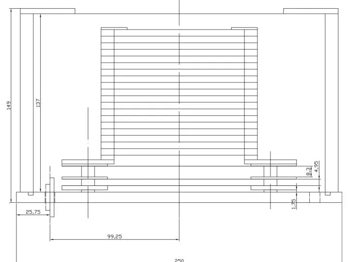
TPC: drift volume of 100 x 100 x 100 mm3. Gas: Ar/Methane 90/10 Drift electrodes: 19 wire loops. Drift voltage: 3000 V. Gas amplification: cascade of 3 GEMs (obtained from F. Sauli). Distance between GEMs: 1.6 mm. E-field: 600 V/mm Distance bottom GEM-MediPix: 6.6 mm. E field: 200 – 400 V/mm At NIKHEF, we operated the chamber using a Cu block instead of the MediPix, and recorded the charge signals on this block. After these signals were understood (eff. gas gains of 2000 – 10000, charge rise time of 150 – 200 ns), we replaced the Cu block by the (operational) MediPix. No signals were observed. On June 26 we repeated the test at CERN where the MediPix experts verified its functioning. It was observed that the analog preamp output (9 pixels have their preamp output connected to the outside world) changed their static baseline when the (single) HV was applied, creating the electric field in the gap between the bottom GEM. This could be explained by a potential change, due to the polarisation of the insulating material, of the gate electrodes. The top metal layer is used for the bumb-bond pads, and for the guard grid between these pads. This reduces the penetration of an E-field into the chip, but maybe not enough. It may also be that the insulating layer on the guard electrode has influence the electric field in the gap between the MediPix and the bottom GEM, causing the electrons not to arrive on the bonding pad Some MediPix chips are being modified. By means of a post process, a metal pad is applied on top of the bonding pad, with dimensions slightly smaller than the pixel dimensions. This will decrease the E-field in the chip, and it reduces the insulating surface of the chip.