Download
1 / 23
230 likes | 341 Views
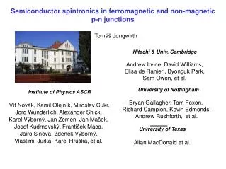
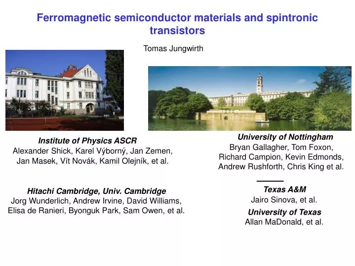
Ferromagnetic semiconductor materials and spintronic transistors. Tom as Jungwirth. Universit y of Nottingham Bryan Gallagher, Tom Foxon, Richard Campion, Kevin Edmonds, Andrew Rushforth, Chris King et al. Institute of Physics ASCR

E N D
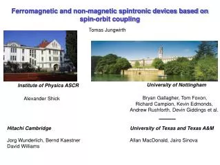
Ferromagnetic semiconductor materials and spintronic transistors Tomas Jungwirth University of Nottingham Bryan Gallagher, Tom Foxon, Richard Campion, Kevin Edmonds, Andrew Rushforth, Chris King et al. Institute of Physics ASCR Alexander Shick, Karel Výborný, Jan Zemen, Jan Masek, Vít Novák,Kamil Olejník, et al. Hitachi Cambridge, Univ. Cambridge Jorg Wunderlich, Andrew Irvine, David Williams, Elisa de Ranieri, Byonguk Park, Sam Owen, etal. Texas A&M Jairo Sinova, et al. University of Texas Allan MaDonald, et al.
Magnetic race track memory Electric field controlled spintronics From storage to logic HDD, MRAM controlled by Magnetic field Spintronic Transistor control by electric gates STT MRAM spin-polarized charge current Low-voltage controlled magnetization and magnetotransport
Outline 1) Sensitivity to electric fields via magnetic anisotropies generic to both metals and semiconductors with spin-orbit coupling - Tunneling AMR device - Coulomb blockade AMR spintronic SET 2) Direct charge depletion effects on electric&magnetic proprties ferromagnetic semiconductors are the favorable systems here - GaMnAs and related dilute-moment ferromagnetic semiconductors - GaMnAs-based p-n junction spintronic FET
Au AMR TMR FM exchange int.: Spin-orbit int.: TAMR FM exchange int.: Discovered in GaMnAs Gould et al. PRL’04
Bias-dependent magnitude and sign of TAMR Shick et al PRB ’06, Parkin et al PRL ‘07, Park et al PRL '08 ab intio theory TAMR is generic to SO-coupled systems including room-Tc FMs experiment Park et al PRL '08
Q SO-coupling (M) VD Source Drain M [010] [110] Gate [100] VG [110] [010] Devices utilizing M-dependent electro-chemical potentials: FM SET magnetic electric & control of Coulomb blockade oscillations
(Ga,Mn)As nano-constriction SET CB oscillations shifted by changing M(CBAMR) Wunderlich et al, PRL '06 Electric-gate controlled magnitude and sign of magnetoresistance spintronic transistor or Magnetization controlled transistor characteristic (p or n-type) programmable logic
Outline 1) Sensitivity to electric fields via magnetic anisotropies generic to both metals and semiconductors with spin-orbit coupling - Tunneling AMR device - Coulomb blockade AMR spintronic SET 2) Direct charge depletion effects on electric&magnetic proprties ferromagnetic semiconductors are the favorable systems here - GaMnAs and related dilute-moment ferromagnetic semiconductors - GaMnAs-based p-n junction spintronic FET
Ga Mn As Mn Ferromagnetic semiconductor GaAs:Mn Jungwirth et al, RMP '06 EF spin ~1% Mn << 1% Mn >2% Mn DOS Energy spin onset of ferromagnetism near MIT As-p-like holes localized on Mn acceptors valence band As-p-like holes As-p-like holes FM due to p-d hybridization (Zener kinetic-exchange) • (Ga,Mn)As: • - heavily-doped SC • difficult to grow and gate • dilute moment FM • difficult to achieve high Tc Mn-d-like local moments
(Ga,Mn)As growth high-T growth optimal-T growth • Low-T MBE to avoid precipitation & high enough T to maintain 2D growth • need to optimize T & stoichiometry for each Mn-doping Detrimental interstitial AF-coupled Mn-donors need to anneal out (Tc can increase by more than 100K) Annealing also needs to be optimized for each Mn-doping
No indication for reaching technological or physical Tc limit in (Ga,Mn)As yet Tc up to 187 K at 12% Mn doping Novak et al. PRL ‘08 2005 Growth & post-growth optimized GaMnAs films 1998
Other (III,Mn)V’s DMSs Kudrnovsky et al. PRB 07 Delocalized holes long-range coupl. Weak hybrid. Mean-field but low TcMF InSb d5 Impurity-band holes short-range coupl. Strong hybrid. Large TcMF but low stiffness GaP GaAs seems close to the optimal III-V host
coupling strength / Fermi energy band-electron density / local-moment density Magnetism in systems with coupled dilute moments and delocalized band electrons Jungwirth et al, RMP '06
Other DMS candidates III = I + II Ga = Li + Zn GaAs and LiZnAs are twin SC (Ga,Mn)As and Li(Zn,Mn)As should be twin ferromagnetic SC • But Mn isovalent in Li(Zn,Mn)As • no Mn concentration limit and self-compensation • possibly both p-type and n-type ferromagnetic SC (Li / Zn stoichiometry) Masek et al. PRL 07
Towards spintronics in (Ga,Mn)As: FM & transport Ordered magnetic semiconductors Disordered DMSs Eu - chalcogenides Broad peak near Tc and disappeares with annealing (higher uniformity)??? Sharp critical contribution to resistivity at Tc ~ magnetic susceptibility
Tc Ni, Fe Eu0.95Cd0.05S Tc
Sharp d/dT singularity in GaMnAs at Tc – consistent with F~d- Novak, et al. PRL‘08
Annealing sequence Optimized GaMnAs materials with x~4-12% and Tc~80-185K: well behaved FMs t=(Tc-T)/Tc
Ga Mn As Mn p s V Beff Strong spin-orbit coupling favorable for spintronics As-p-like holes Strong SO due to the As p-shell(L=1) character of the top of the valence band
Low-voltage gating of the highly doped (Ga,Mn)As 10’s-100’s Volts in conventional MOS FETs Ohno et al. Nature ’00, APL ‘06 p-n junction FET p-n junction depletion simulations 2x 1019 cm-3 ~25-50% depletion feasible at low voltages Owen, et al. arXiv:0807.0906
Basic charcteristics of the device can “deplete” magnetization at low Vg can deplete charge at low Vg low Vg dependent competition of uniaxial and cubic anisotropies 30% AMR tuneable by low Vg
Ga Mn As Mn Conclusion 1) Studies in GaMnAs suggest new generic approaches to electric field controlled spintronics via magnetic anisotropies - TAMR - CBAMR 2) Direct charge depletion effects on electric&magnetic properties of GaMnAs demonstrated at low gate voltages - GaMnAs junction FET