Download
1 / 91
990 likes | 1.35k Views
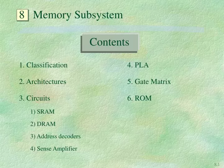
Contents. 8 Memory Subsystem. 1. Classification 2. Architectures 3. Circuits 1) SRAM 2) DRAM 3) Address decoders 4) Sense Amplifier. 4. PLA 5. Gate Matrix 6. ROM. 1. Classification. RWM(Read-Write Memory) Random Access : SRAM, DRAM Sequential Access : FIFO, Stack(LIFO)

E N D
Contents 8 Memory Subsystem 1. Classification 2. Architectures 3. Circuits 1) SRAM 2) DRAM 3) Address decoders 4) Sense Amplifier 4. PLA 5. Gate Matrix 6. ROM
1. Classification • RWM(Read-Write Memory) • Random Access : SRAM, DRAM • Sequential Access : FIFO, Stack(LIFO) • Content Access : CAM(Associative Memory) • NVRWM(Nonvolatile RWM) • EPROM • E2PROM • FLASH • ROM • Mask Programmed • OTP(One-Time Programmable) ; PROM
2. Architectures • 1-dimensional memory : N(words) M(bits/word) • Decoder reduces the number of wires
2-dimensional array structure uses column decoder to make the chip square.
Hierarchical memory architecture using block address • Block address is used to activate only one block. Other blocks(nonactive) are put in power-saving mode.
Another schematic of SRAM(column grouping). SRAM chip block diagram
Design Considerations • bit line precharge, sense amp enable 등을 위한 모든 clock의 발생은 address, CS, WE 등 신호의 transition을 detect하는 회로에 의해 internal clock 발생기가 trigger 됨으로써 이루어진다.(전력소모 억제) • 2-stage row address decoding : WL driver decodes A1. • Sense amp는 column switch 앞에, 혹은 뒤에 놓을 수 있다. 앞에 놓을 경우 : column의 cell pitch에 맞추기 위해 아주 simple한 SA를 사용 뒤에 놓을 경우 : 상대적으로 복잡한 SA 사용가능(SA의 input cap.는 증가 • 윗 그림은 column을 (1024 column의 경우, by 4 인 경우) 크게 4로 나누고, 각각을 16으로 나누어 각 소 group의 16개의 column을 한 SA가 담당토록하는 compromise 임.
3. Circuits • Address decoders • Single stage(10-to-1024) decoder i) # of transistors = 20/NAND 10 1024 = 20,480 ii) Large fanout requirement on buffers generating Xi’s. iii) series-connected transistors limit discharge time.
Predecoded scheme i) Group 2 bits and predecode the word using 2-bit segments ; (X9, X8), (X7, X6), …. (X1, X0) ii) 2nd-stage decoder logic # of transistors ; 10/NAND 5 1024 + 12,000
Divided Word Line architecture Global word line selects a block, while the local line is used to activate a word line within the selected block.
Row decoder circuits (Complementary AND, pseudo NMOS, cascade NAND)
Various other decoder circuits(Power saving, Decoder-powered)
Sense Amplifier for SRAM • Single differential stage의 전압이득 Av = gm·ro gm : current/voltage(transducer gain) of M1, M2 ro : output impedance( = ro M1 ro M2) • Av가 크기 위해서는 M1과 P1(M2와 P2)가 모두 saturation 영역에 있어야 함. ( Sat. 영역에서 gm= 가 크고, ro도 크기때문) • 따라서 point X의 전압을 로 precharge해 두는 것이 response time을 짧게 하고, signal swing을 크게하는데 유리.
Single-ended amp를 두개 symmetric하게 연결함으로써 voltage gain을 높인다. (다음 단에 latch나 another double-ended amp. Stage 혹은 diff. Input을 갖는 output buffer를 달면 된다.)
SA의 출력점을 로 충전하여 SA의 high-gain 영역에서 동작토록하는 회로. 1 : V1은 VDD로 prech 됨 power-down 상태 2 : WL이 access되면 V1을 로 prech. 3 : BL, BL에 전압차가 생기면 high-gain SA 동작하면서 column decoder/switch인 pass gate가 동작 data output bus로 신호전달 4 : power-down 상태 • SRAM sense amp precharged to
Evolution of SRAM cells i) 6- and 4-transistor SRAM cells
ii) Dual-port/double-ended access and dual-port/single access
Evolution of DRAM cells (a) basic bi-stable f/f w/o load (b) 2C-2D(C:control lines, D:data lines)
Cross-coupled Latch Assume node 1 & 2 are precharged, and node 2 begins to drop. When clk is on, node 3 pulls down. N2 strongly turns on, leaving n1 off. 주의) cross-coupled TR pair 의 layout이 대칭이어야 함. threshold 전압차이에 의한 영향
Charge-transfer Circuit(cont’d) • Operation Sequence As clk goes high, node 1 & 2 are precharged; V1 (Vref-Vth,n2), V2 min(VDD, Vclk-Vth, n3) > Vref n3 turns off. Cell(n1, Cc) is selected(Assume Vc was ‘0’) Due to charge sharing between Cc & Clarge, V1 becomes n2 is turned on until is transferred from Cout .i.e., until V1 reaches Vref-Vth. Voltage drop at node 2 due to charge transfer is : amplif. factor
Sense amplifier for single - Tr. DRAM cells. dummy cell(Cd=Cc), dummy bit line complete Symmetry
Operation 1. Precharge 전에는 BL, DBL 모두 로 되어 있다.* precharge(n1, n2 on)를 통해 node 1,2가 pull up 된다. 그리고 n1과 n2는 off된다. 2. Cc와 Cd가 select 되어 charge transfer에 의해 ( =0라 하자) node 1의 전압은 node 2의 전압보다 많이 강하 된다. ( Cd는 로 충전되어 있었기 때문)* 3. Clk1이 high가 되어 n4는 on, n5는 off(V1은 Vss로 됨) n7이 다시 conduction 되어 BL이 Vss로 방전되어 Cc가 ‘0’으로 restore 된다. 4. Sel ‘0’로 하여 Cc를 isolate 한 후에 clk2를 on하여 BL과 DBL을 로 함. 그 후에 seld ‘0’ 하여 Cd에 를 만들고 n3를 off 시킴. (Cc에 ‘1’이 저장되어 있는 경우도 비슷한 방식으로 동작한다.)
Column SA와 main SA를 사용한 SRAM SA 회로 매 column마다 n개의 colunm간에 multiplex
(input 신호) (Column SA가 있는 경우)
Resistive-load SRAM cells • Undoped polysilicon as resistors with R 1 / • Just enough(10-12A) to compensate for leakage current of 10-15A • BL & BL precharged to VDD, thus preventing slow charging of BL, BL.
TFT SRAM cell • Instead of traditional PMOS devices, pull-up transistors realized by PMOS TFT(thin-film transistor) on top of the cell structure. • ON current : 10-8A, OFF current : 10-13A Complementary CMOS Resistive Load TFT cell Number of transistors 6 4 4(+2 TFT) Cell size 58.2m2 (0.7 m rule) 40.8 m2 (0.7 m rule) 41.1m2 (0.8 m rule) Standby current(per cell) 10-15A 10-12A 10-13A
Bipolar SRAM cells : • Very fast SRAMs are necessary for cache & microcode memory in high-speed computers. • SBD(Schottky Barrier Diode) bipolar SRAM
3-T DRAM cell : • Resulted by removing the loads to obtain 4-T DRAM cell and further removing redundemt complementary pull down device • Separate Read Word line(RWL) & Write word line(WWL) • Refreshing by writing the inverted BL2 signal onto BL1.
1-T DRAM cell : : charge transfer ratio