Download
1 / 9
90 likes | 239 Views
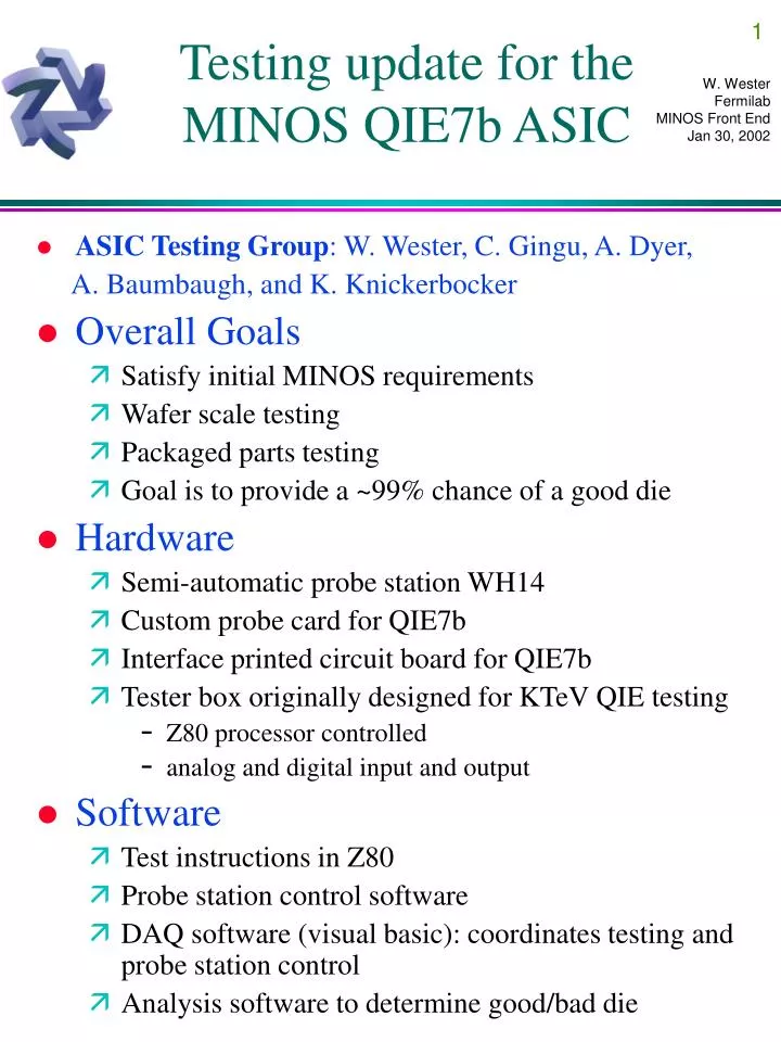
Testing update for the MINOS QIE7b ASIC. ASIC Testing Group : W. Wester, C. Gingu, A. Dyer, A. Baumbaugh, and K. Knickerbocker Overall Goals Satisfy initial MINOS requirements Wafer scale testing Packaged parts testing Goal is to provide a ~99% chance of a good die Hardware

E N D
Testing update for theMINOS QIE7b ASIC • ASIC Testing Group:W. Wester, C. Gingu, A. Dyer, A. Baumbaugh, and K. Knickerbocker • Overall Goals • Satisfy initial MINOS requirements • Wafer scale testing • Packaged parts testing • Goal is to provide a ~99% chance of a good die • Hardware • Semi-automatic probe station WH14 • Custom probe card for QIE7b • Interface printed circuit board for QIE7b • Tester box originally designed for KTeV QIE testing • Z80 processor controlled • analog and digital input and output • Software • Test instructions in Z80 • Probe station control software • DAQ software (visual basic): coordinates testing and probe station control • Analysis software to determine good/bad die
48 wafer production has arrived! Approx 699 chips per wafer (33.5K parts) Initial goal: Begin delivery of ~1250 known good die (KGD) by mid Feb for assembly of MENU modules for the test beam. The QIE7b ASIC for MINOIS Clk Ref Input Four phase Integrator digital circuitry Current Splitter Sig Output Sig Input Exp Cap ID
Wafer testing before packaging • Somewhat of an academic exercise • Testing after packaging can be done anyway • Some potential benefits • Quicker initial look • Study process variations versus wafer position • Higher statistics for determining pass/fail criteria • After chip packaging more efficient • Maybe only wafer testing (saves ~2 months!) Example of wafer testing result that shows chips that pass testing but reside in a bad area on the wafer CDF DDR device
Testing on the wafer • Procedure • Place wafer on the chuck and align • Start probe station soft-ware • Some Problems • Higher noise than with packaged parts • Some system glitches we’re tracking down • Each part gets tested 3 times for now • 2000 parts per day with ~3 hrs work
Testing after packaging • QIE5b tested in this manner by KTeV • SMQIE tested in this manner by CDF • Procedure: • Insert packaged part into a clam shell • Press a button • Read pass/fail based upon a LED readout • Some difficulties • Clam shells require periodic cleaning • Human error always a possibility • About 2 chips can be tested per min or 1000/day
Test sequence • Nearly identical for wafer testing or for testing after packaging. • Developed originally for the KTeV QIE • Used for other QIE versions as well • Check functionality and perform measurements • Power-on current measurement (2 supplies) • Cap Ids rotating? • Pull current out through input ref • Inject current and see all 8 exponent ranges • Pedestal values (analog out is digitized) • Look at AC/DC “impedence” (input voltage) • Measure Aout (2 points in each range) • Measure LVDS voltage levels for Cap ID and exponent lines for high and low
Test data • Output of testing data is a text file with 43 lines per device. Also in .paw files • Visual Basic and Linux fortran analysis • Web site will be set up 00STATUS F 1 1 0 0 1 1 2 2 3 3 4 4 5 5 6 6 7 7 01 071007 001907 002907 006806 17B006 179F06 178904 37BF04 557804 455004 5FCB04 353804 637104 2AAC04 622604 24B904 5FAF04 221904 5FB504 1B2304 4FF904 282804 57570A 328E0A 328F0A 32890A 32890B 34840B 30BD0B 34840B 30B30B 34850B 30A40B 30BA0B 34840B 30B30B 34830B 30A30B 34840D 49500D 4C8D Status and range exponents Aout for pedestal Range 7 Aout at ~20% full range Range 7 Aout at ~80% full range LVDS low voltage LVDS high voltage 12 V supply current 6V supply current
Some Results Wafer 05 636/699 die good 91% yield Failures mostly at the wafer’s edge Wafer 08 628/699 die good 90% yield 3 additional wafers tested with similar results
Long and short term goals • Two wafers have been tested: 90% yield! • Bad die are inked and won’t be packaged • Packaging at ASAT (two wafers are now in Hong Kong). Should return by mid-Feb. with ~1250 good packaged parts • When parts arrive, they will be tested after packaging to determine whether additional failures are introduced or to perhaps to further select more uniform devices • Based upon our findings, we will decide whether packed part testing is needed for the remainder of the parts • Wafer testing to be finished by ~May