Download
1 / 10
100 likes | 251 Views
VMM Update Front End ASIC for the ATLAS Muon Upgrade. V. Polychronakos BNL. Design Parameters/Features. Dual Polarity Adjustable Gain (0.5 – 9.0 mV/ fC ) Adjustable peaking Time (25-200 ns) Address in Real Time (Fast OR in effect - Mmegas Trigger)

E N D
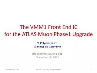
VMM UpdateFront End ASIC for the ATLAS Muon Upgrade V. Polychronakos BNL nSW Electronics Workshop - V. Polychronakos, BNL
Design Parameters/Features • Dual Polarity • Adjustable Gain (0.5 – 9.0 mV/fC) • Adjustable peaking Time (25-200 ns) • Address in Real Time (Fast OR in effect - Mmegas Trigger) • Prompt digitized (6-bit) Amplitude, Time-over-threshold, time-to--peak (TGC Trigger) • Peak Detector, Time Detector (<1 ns) • Discriminators with sub-hysteresis • Neighbor enable logic (channel to channel and across Ics) • Sparse readout w/smart token passing, • Threshold trim, built-in calibration, channel mask, analog monitor, temp. sensor, 600 BGR, 600 mV LVDS nSW Electronics Workshop - V. Polychronakos, BNL
VMM1, First Version, 64 channels, fully functional analog front end, Amp, Timing analog multiplexer outputs nSW Electronics Workshop - V. Polychronakos, BNL
The Second version of the ASIC (VMM2) • Fixes issues (mostly minor) of the first version • Includes 10-bit digitizers for amplitude and timing (200 ns) • Includes a 6-bit Amplitude digitizer at ~40 ns conversion time • Includes 4 word buffer, simultaneous read/write, can continuously be read out at both phases of 200 MHz clock in DDR mode 800 Mbps G. De Geronimo, BNL Instr. Div. IBM 8RF 130 nm CMOS process, 1.2 V 9.1 x 9.1 mm2, ~6.5 mW/channel nSW Electronics Workshop - V. Polychronakos, BNL
VMM2 Readout (May be modified in final version) 4-deep buffer 200 MHz Clock Uses both phases Effectively 800 Mbps nSW Electronics Workshop - V. Polychronakos, BNL
Trigger Feature 1- Address in Real Time (ART) At every bunch crossing ART provides the 6-bit address of the channel with the earliest signal above threshold Can be used as a fast OR nSW Electronics Workshop - V. Polychronakos, BNL
Trigger Feature 2- Prompt 6-bit amplitude per Channel nSW Electronics Workshop - V. Polychronakos, BNL
Summary, Schedule - Availability • VMM2 design completed about a month ago • Layout, simulations in progress, expect to be completed end of November (next MOSIS MPW run) • VMM is a very large chip (> 100 sq.mm), cost 230 k$US/40 samples! • Decided to go for a dedicated run (450 k$US) sharing the wafer with a smaller BNL ASIC which will reduce the cost by ~ 100 k • The cost above includes processing of 6 wafers, ~600-700 chips • Chips available ~May 2014 if submitted in early December • Package in BGA 350 pins (21x21 mm2) • In the process of applying for Commerce Department export license • What remains for the final version is SEU mitigation logic and final decision on digital buffer size and management • Several Readout boards for ATLAS under development, SRS compatible hybrid under discussion nSW Electronics Workshop - V. Polychronakos, BNL
IBM 8RF-DM Reticule 20x18 mm2 20 mm 18 mm nSW Electronics Workshop - V. Polychronakos, BNL
Some consequences of the dedicated runs, • and the relative size of the VMM and reticule • Only 2 VMM fit in a reticule • 60 reticules per 8-inch wafer • 110 chips/wafer (90% yield) • Need to produce 450 wafers not 250 as in the current plan • This is an additional 400 k$ • But have more room for additional ASICs • Additional ASIC prototypes can be done for free • Any run could be the “production run” • Digital chips need to catch up fast! Otherwise no savings in co- • production • Common production IC for both detectors • (recall discussions of dedicated layouts for sTGC and Mmegas) • This is OK but maybe different BGA substrates? • Needs to be studied, weigh advantages vs additional ~40 k$ for a • second substrate nSW Electronics Workshop - V. Polychronakos, BNL