Download
1 / 34
450 likes | 820 Views
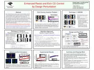
Comprehensive CD Uniformity Control in Lithography and Etch Process. Qiaolin Zhang a, Cherry Tang b , Tony Hsieh b , Nick Maccrae b , Bhanwar Singh b , Kameshwar Poolla a , Costas Spanos a a Dept of EECS, UC Berkeley b SDC, Advanced Micro Devices March 3, 2005. Motivation.

E N D
Comprehensive CD Uniformity Control in Lithography and Etch Process Qiaolin Zhanga, Cherry Tangb, Tony Hsiehb, Nick Maccraeb, Bhanwar Singhb, Kameshwar Poollaa, Costas Spanosa aDept of EECS, UC Berkeley bSDC,Advanced Micro Devices March 3, 2005
Motivation • Importance of across-wafer (AW) CD (gate-length) uniformity • Impacts IC performance spread and yield • Large AW CDV large die-to-die performance variation low yield • How to cope with increasing AW CD variation? • Employ design tricks, ex. adaptive body biasing • Has limitations • Reduce AW CD variation during manufacturing • The most effective approach
PEB Develop Spin/Coat Total across-wafer CD Variation Etch Exposure Deposition Across-wafer CD Variation Sources
Spin/ Coat/ PAB Exposure PEB Develop Etch Optimal zone offsets Optimizer CD Metrology CD Uniformity Control Approach • Current litho clusters strive for uniformPEB profile of multi-zone bake plate and contemplate die-to-die exposure dose compensation to improve CDU. • Our approach is to manipulate across-wafer PEB profiles to compensate for other systematic across-wafer poly CD variation sources
6 3 1 5 7 2 4 PEB Bake Plate Zone offset knobs Multi-zone PEB Bake plate Schematic setup of multi-zone bake plate (approximate) Each zone is given an individual steady state target temperature, by adjusting an offset value
Develop Inspection (DI) CDU Control Methodology • The across-wafer DI CD is a function of zone offsets • Seen as a constrained nonlinear programming problem • Minimize • Subject to:
Snapshot of Derived CD-to-Offset Model • Empirically derived CD-to-offset modelbased on temperature-to-offset model and resist PEB sensitivity Zone 1 Zone 2 Zone 3 Zone 4 Zone 5 Zone 6 Zone 7 nm/offset unit
Simulation Results of DI CDU Control Dense Line Semi-isolated Line Isolated Line Experimentally extracted baseline CDU Simulated optimal CDU after applying DI CDU control
Now we minimize: Final Inspection (FI) CDU Control Methodology • Across-wafer FI CD is function of zone offsets • Plasma etching induced AW CD Variation (signature) • Subject to:
Plasma Etching Induced AW CD Variation • PEB-based DI control can be tuned to anticipate the plasma induced non-uniformity and cancel it. • Use 3 plasma non-uniformity examples to simulate the proposed FI CDU control approach. Bowl Dome Tilt
FI CDU Control Simulation - Bowl Plasma Signature Dense Semi-isolated Isolated Experimentally extracted baseline CDU Simulated corrected DI CD after applying FI CDU control Simulated optimal FI CD after applying FI CDU control
FI CDU Control Simulation - Dome Plasma Signature Dense Semi-isolated Isolated Experimentally extracted baseline CDU Simulated corrected DI CD after applying FI CDU control Simulated optimal FI CD after applying FI CDU control
FI CDU Control Simulation - Tilted Plasma Signature Dense Semi-isolated Isolated Experimentally extracted baseline CDU Simulated corrected DI CD after applying FI CDU control Simulated optimal FI CD after applying FI CDU control
Simultaneous CDU Control for Multiple CD Targets • Multi-objective optimization of CDU for multiple targets • Minimize the weighted sum of deviation of each target • Subject to: • Optimal zone offsets: • The relative magnitude of the weighting factor indicates the importance of meeting the corresponding CD target
Simultaneous CDU Control for Multiple CD Targets • What is the best improvement possible for multiple targets? • How can we automatically find the corresponding weighting factors and optimal zone offsets? • Minimax optimization • Weighting factors of the jth iteration along the optimal searching trajectory: • Minimaxto find optimal weighting factors and offsets
Simultaneous CDU Control for Multiple CD Targets Simulation of simultaneous CDU control for dense, semi-iso and iso lines Dense Semi-isolated Isolated Experimentally extracted baseline CDU Simulated optimal FI CD after applying simultaneous CDU control
Summary and Conclusions • Extracted CDU signatures of dense, iso and semi-iso • CD-to-offset model enables DI & FI CDU control • The derived CD-to-offset model is based on temperature-to-offset model and resist PEB sensitivity • Offers better fidelity than the old CD-to-offset model purely based on CD measurement • Simulation indicates promise of DI & FI CDU control • Multi-objective & minimax optimization schemes enable simultaneous CDU control for multiple CD targets • Work in SDC at AMD are under way to validate this approach experimentally
Technology/Circuit Co-Design:Impact of Spatial Correlation Paul Friedberg Department of Electrical Engineering and Computer Sciences University of California, Berkeley Feb. 14, 2005
Outline • Motivation • Spatial Correlation Extraction • Impact of Spatial Correlation on Circuit Performance • How does process control impact spatial correlation? • Conclusions/Future Plans
Circuit design Manufacturing Gate length, Vth, tox power performance Motivation: reality design rules
Canonical circuit Manuf. statistics μ, σ, ρ power performance Motivation: simulation primary focus: spatial correlation
Spatial Correlation Analysis • Exhaustive ELM poly-CD measurements (280/field): • Z-score each CD point, using wafer-wide distribution: • For each spatial separation, calculate correlation ramong all within-field pairs: (CD data courtesy of Jason Cain)
Spatial Correlation Dependence • Within-field correlation vs. horizontal/vertical distance, evaluated for entire wafer: • Statistical assumptions are violated (distribution is not stationary): we will address this later
Ignore this part of the curve— restrict critical paths to some reasonable length rB Characteristic “correlation baseline” XL, characteristic “correlation length” Spatial Correlation Model • Fit rudimentary linear model to spatial correlation curve extracted from empirical data:
100 mm 100m Input Stage i Output Monte Carlo Simulations • Use canonical circuit of FO2 NAND-chain w/ stages separated by 100mm local interconnect, ST 90nm model: • Perform several hundred Monte Carlo simulations for various combinations of XL, rB, and s/m (gate length variation) • Measure resulting circuit delays, extract normalized delay variation (3s/m )
25 XL scaling 20 L scaling Normalized delay variability (3/) (%) 15 B = 0.4 B = 0.2 10 B = 0.0 0% 20% 40% 60% 80% 100% 5 Scaling factor Delay Variability vs. XL, rB, s/m • Scaling gate length variation directly: most impactful • Reducing spatial correlation also reduces variability, increasingly so as r decreases
Spatial components CDij = + mask + fi + wj + εij True mean Across-wafer Across-field Origin of Spatial Correlation Dependence • CD variation can be thought of as nested systematic variations about a true mean: Wafer Field
- = Slit Scan Non-mask related across-field systematic variation Scaled Mask Errors Average Field Origin of Spatial Correlation Dependence • Within-die variation: Removing this component of variation will simulate WID process control Polynomial model of across-field systematic variation
Origin of Spatial Correlation Dependence • Across-wafer variation extraction: - - Average Wafer Scaled Mask Errors Across-Field Systematic Variation Removing this component of variation will simulate AW process control = Across-Wafer Systematic Variation Polynomial Model
Artificial WID Process Control • By removing the within-field component of variation, we get distinctly different correlation curves: • Shape of curve changes; correlation decreases for horizontal, but increases for vertical
Artificial AW Process Control • Removing the across-wafer component only: • Shape stays roughly the same; correlation decreases across the board
Artificial AW+WID Process Control • Removing both AW and WID components, get a cumulative effect larger than the sum of the parts:
Additional process control • One more round of control: die-to-die dose control - = Horizontal separation Vertical separation
Conclusions • Correlation effects are significant: should definitely be included in MC simulation frameworks • Spatial correlation virtually entirely accounted for by systematic variation Complete process control can almost completely reconcile correlation • As process control is implemented, σ and ρ are simultaneously reduced: a double-win • The closer to complete control, the greater the impact of additional control on correlation • Last “little bit” of systematic variance in the distribution causes substantial correlation