Download
1 / 27
270 likes | 472 Views
Chapter 20 Quasi-Resonant Converters. Introduction 20.1 The zero-current-switching quasi-resonant switch cell 20.1.1 Waveforms of the half-wave ZCS quasi-resonant switch cell 20.1.2 The average terminal waveforms 20.1.3 The full-wave ZCS quasi-resonant switch cell

E N D
Chapter 20Quasi-Resonant Converters • Introduction • 20.1 The zero-current-switching quasi-resonant switch cell 20.1.1 Waveforms of the half-wave ZCS quasi-resonant switch cell 20.1.2 The average terminal waveforms 20.1.3 The full-wave ZCS quasi-resonant switch cell • 20.2 Resonant switch topologies 20.2.1 The zero-voltage-switching quasi-resonant switch 20.2.2 The zero-voltage-switching multiresonant switch 20.2.3 Quasi-square-wave resonant switches • 20.3 Ac modeling of quasi-resonant converters • 20.4 Summary of key points
The resonant switch concept • A quite general idea: • 1. PWM switch network is replaced by a resonant switch network • 2. This leads to a quasi-resonant version of the original PWM converter Example: realization of the switch cell in the buck converter
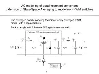
Two quasi-resonant switch cells Insert either of the above switch cells into the buck converter, to obtain a ZCS quasi-resonant version of the buck converter. Lr and Cr are small in value, and their resonant frequency f0 is greater than the switching frequency fs.
20.1 The zero-current-switchingquasi-resonant switch cell • Tank inductor Lr in series with transistor: transistor switches at zero crossings of inductor current waveform • Tank capacitor Cr in parallel with diode D2 : diode switches at zero crossings of capacitor voltage waveform • Two-quadrant switch is required: • Half-wave:Q1 and D1 in series, transistor turns off at first zero crossing of current waveform • Full-wave:Q1 and D1 in parallel, transistor turns off at second zero crossing of current waveform • Performances of half-wave and full-wave cells differ significantly.
Averaged switch modeling of ZCS cells • It is assumed that the converter filter elements are large, such that their switching ripples are small. Hence, we can make the small ripple approximation as usual, for these elements: In steady state, we can further approximate these quantities by their dc values: • Modeling objective: find the average values of the terminal waveforms • v2(t) Ts and i1(t) Ts
The switch conversion ratio µ A generalization of the duty cycle d(t) The switch conversion ratio µ is the ratio of the average terminal voltages of the switch network. It can be applied to non-PWM switch networks. For the CCM PWM case, µ = d. If V/Vg = M(d) for a PWM CCM converter, then V/Vg = M(µ) for the same converter with a switch network having conversion ratio µ. Generalized switch averaging, and µ, are defined and discussed in Section 10.3. In steady state:
20.1.1 Waveforms of the half-wave ZCSquasi-resonant switch cell The half-waveZCS quasi-resonant switch cell, driven by the terminal quantitiesáv1(t)ñTs and ái2(t)ñTs. Waveforms: Each switching period contains four subintervals
Circuit equations: with i1(0) = 0 Solution: where Subinterval 1 Diode D2 is initially conducting the filter inductor current I2. Transistor Q1 turns on, and the tank inductor current i1 starts to increase. So all semiconductor devices conduct during this subinterval, and the circuit reduces to: This subinterval ends when diode D2 becomes reverse-biased. This occurs at time w0t = a, when i1(t) = I2.
Subinterval 2 Diode D2 is off. Transistor Q1 conducts, and the tank inductor and tank capacitor ring sinusoidally. The circuit reduces to: The solution is The dc components of these waveforms are the dc solution of the circuit, while the sinusoidal components have magnitudes that depend on the initial conditions and on the characteristic impedance R0. The circuit equations are
Subinterval 2continued Peak inductor current: This subinterval ends at the first zero crossing of i1(t). Define b = angular length of subinterval 2. Then Hence Must use care to select the correct branch of the arcsine function. Note (from the i1(t) waveform) that b > p.
Boundary of zero current switching If the requirement is violated, then the inductor current never reaches zero. In consequence, the transistor cannot switch off at zero current. The resonant switch operates with zero current switching only for load currents less than the above value. The characteristic impedance must be sufficiently small, so that the ringing component of the current is greater than the dc load current. Capacitor voltage at the end of subinterval 2 is
Subinterval 3 All semiconductor devices are off. The circuit reduces to: Subinterval 3 ends when the tank capacitor voltage reaches zero, and diode D2 becomes forward-biased. Define d = angular length of subinterval 3. Then The circuit equations are The solution is
Subinterval 4 Subinterval 4, of angular length x, is identical to the diode conduction interval of the conventional PWM switch network. Diode D2 conducts the filter inductor current I2 The tank capacitor voltage v2(t) is equal to zero. Transistor Q1 is off, and the input current i1(t) is equal to zero. The length of subinterval 4 can be used as a control variable. Increasing the length of this interval reduces the average output voltage.
Maximum switching frequency The length of the fourth subinterval cannot be negative, and the switching period must be at least long enough for the tank current and voltage to return to zero by the end of the switching period. The angular length of the switching period is where the normalized switching frequency F is defined as So the minimum switching period is Substitute previous solutions for subinterval lengths:
20.1.2 The average terminal waveforms Averaged switch modeling: we need to determine the average values of i1(t) and v2(t). The average switch input current is given by q1 and q2 are the areas under the current waveform during subintervals 1 and 2. q1 is given by the triangle area formula:
Charge arguments: computation of q2 Node equation for subinterval 2: Substitute: Second term is integral of constant I2: Circuit during subinterval 2
Charge argumentscontinued First term: integral of the capacitor current over subinterval 2. This can be related to the change in capacitor voltage : Substitute results for the two integrals: Substitute into expression for average switch input current:
Switch conversion ratio µ Eliminate a, b, Vc1 using previous results: where
Analysis result: switch conversion ratio µ Switch conversion ratio: with This is of the form
Characteristics of the half-wave ZCS resonant switch Switch characteristics: Mode boundary: Js ≤ 1
Buck converter containing half-wave ZCS quasi-resonant switch Conversion ratio of the buck converter is (from inductor volt-second balance): For the buck converter, ZCS occurs when Output voltage varies over the range