Download
1 / 39
400 likes | 527 Views
Degradation in MOSFET Multi-Stack High-k Gate Dielectrics Due to Hot Carrier and Constant Voltage Stress. Z. Celik-Butler and M. S. Rahman. The Nanotechnology Research and Teaching Facility, Electrical Engineering Department University of Texas at Arlington, Arlington, TX 76019.

E N D
Degradation in MOSFET Multi-Stack High-k Gate Dielectrics Due to Hot Carrier and Constant Voltage Stress Z. Celik-Butler and M. S. Rahman The Nanotechnology Research and Teaching Facility, Electrical Engineering Department University of Texas at Arlington, Arlington, TX 76019
Outline • Motivation for / Significance of High-k Dielectrics • Low – Frequency Noise • Importance • Current Models • MSUN Model • Effect of Nitridation on 1/f Noise • Effect of Nitridation on Stress Induced Degradation • Summary
The ITRS Road Map Power trends § §2007 Roadmap ± High-k is needed to reduce leakage current High-k is needed to enable manufacturing ±2005 Roadmap
Motivation for High-k Gate Dielectric Materials-I Power Consumption in Digital CMOS • Standby Power • Power when no function is occurring. • Critical for battery driven. • Can be reduced through circuit optimization • Temperature dependent leakage current. • Active Power • Switching power plus passive power. • Critical for high performance applications. • Other Sources of Power Consumption • Analog and I/O power. • Dynamic memory refresh power.
Motivation for High-k Gate Dielectric Materials-II § Problems associated • Fixed charges • Compatibility with gate material • Interfacial layer • Charge trapping • Threshold voltage instability • Mobility degradation ±M. Bohr et al, IEEE Spectrum, pp.30-35, Oct 2007 §http://www.intel.com/technology/silicon/high-k.htm?iid=search
Candidates for High-k Gate Dielectric Materials Dielectric constant • Most Suitable value: 7~35 Very high : causes FIBL Very low : difficult to decrease Ig Interface state/Oxide trap charge density • Comparable with SiO2 (~1010 /eV.cm2) Thermal stability J Robertson, et al J. V. S. T. B v. 18(3), 1785 (2000) • Endurance up to ~700oC Hafnium Silicon Oxide • High dielectric constant and large bandgap (Eg=5.68eV) • Thermally stable in contact with silicon. • Close lattice matching with silicon (a= 5.11Ao a-Si=5.43Ao). • Can be wet etched by HF acid.
Challenges in Implementation of High-k Materials • The incorporation of the high-k materials greatly decreases the leakage current, but introduces the following drawbacks: • Charge trapping in the dielectric • Lower carrier mobility • Threshold voltage instability • Soft optical phonon scattering • Higher low frequency 1/f noise
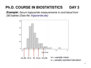
Low Frequency Noise: Significance • Also known as 1/f noise or flicker noise • Dominant source of noise for f<10KHz • The power spectral density is characterized by 1/fδ with δ between 0.7 and 1.4 • Serves as a figure-of-merit for the reliability and stability issues of semiconductor devices • Sets the limit for the achievable dynamic range (signal to noise ratio) for baseband/LF circuits • An important design constraint for RF and microwave circuits as it gets modulated to HFs
Introduction to Low-Frequency Noise Models • Unified Noise Model (UN Model):‡ • Successful for native oxide MOSFETs • Based on dielectric trap induced correlated number and mobility fluctuation • Incorporated into BSIM and PSP simulators. • Discrepancies in applying UN to high-k MOSFET devices: ♯ • Extracted trap density values differ even for the same material and process. • Extracted trap density values show dependence on interfacial layer thickness which is not a model parameter. • ‡ K.K. Hung et al. IEEE Trans. Electron Devices 37, 654 (1990). • ♯ Z. Çelik-Butler. Proc SPIE fluctuations and noise 2006 5844, 177.
z L x W SiO2 Tox y Traps Source Drain Substrate Carriers Physical Mechanisms for LF Noise in MOSFETs Channel carriers tunnel back and forth from the traps in the gate oxide causing fluctuations in the number of carriers. By virtue of Coulomb scattering from oxide trapped charges there are fluctuations in carrier mobility that cause additionalnoise in correlation with the carrier number fluctuations. K. K. Hung, P. K. Ko, C. Hu, Y. C. Cheng, “A unified model for the flicker noise in metal-oxide-semiconductor field-effect transistors,” IEEE Trans. Electron Devices, vol. 37, pp.654-665, 1990.
Unified Flicker Noise Model: Assumptions • Correlated carrier number and surface-mobility fluctuations • Equi-energy tunneling process • Traps in the gate dielectric trap/de-trap channel carriers • Trapping/de-trapping phenomenon causes fluctuations in the carrier number • Fluctuations in carrier mobility in correlation to the carrier number fluctuation • Uniform distribution of traps in the gate dielectric with respect to distance and energy level
The Unified Noise Model • Correlated number and mobility fluctuation theory predicts1 repulsive trap-carrier interactions • PSD for fluctuation in the trapped carriers is given by: • Simplifications : only traps at the Fermi level are active uniform trap density/ infinitely thick dielectric • The total drain current noise power becomes • The resultant noise is always pure 1/f
z L x THK W High-k y TIL Traps x y z Source Drain Substrate Carriers Interfacial layer Noise Mechanisms in High-k Gate Stack Channel carriers tunnel into the traps in high-k and interfacial layer causing fluctuations in carrier number and mobility in a correlated way. The uniform dielectric trap density assumption does not hold. The different trap profiles and various physical properties of high-k/interfacial layer materials like physical thicknesses, barrier heights etc. affect the 1/f noise.
Why Doesn’t UFN Model Work for High-κ MOSFETs? • High-κ gate MOSFETs differ in many respects from their native oxide (SiO2) counter-parts, for which the Unified Model was developed : • Higher trap densities compared to SiO2.1 • Multilayered gate stack2 compared to single layer of SiO2. • Spatial3 and energy dependence4 of active trap densities. • Carrier mobility degradation by remote phonon scattering5. 1 B. Min; et al. IEEE Trans Electron Dev 51, 1679 (2004). 2 G.D. Wilk; et al. J Appl Phys89, 5243 (2001). 3 Z. Celik-Butler; et al. IEEE Trans Electron Dev 35, 1651 (1988) 4P. Srinivasan; et al. J Electrochem Soc 153, G819 (2006). 5M. V. Fischetti; et al. J Appl Phys 90, 4587 (2001)
The Multi-Stack Unified Noise (MSUN) Model: Assumptions♦ • A new flicker noise model for high-κ dielectric MOSFETs • Based on the correlated number and surface mobility fluctuation model (Unified Flicker Noise Model) • Equi-energy tunneling of charge carriers in the dielectric • Scalable with regards to the high-κ/interfacial layer physical thicknesses • Takes different dielectric material properties into account • Considers non-uniform distribution of traps in the high-κ /interfacial layer with respect to distance and energy level • T. Morshed, M. S. Rahman et al.IEDM Tech. Dig., 2007, pp. 561-564.
Total Noise Power spectral density of the mean square fluctuations in the number of occupied trapsfor high-k/interfacial layer stack Z. Çelik-Butler, “Different noise mechanisms in high-k dielectric gate stacks,” in Proc. SPIE—Noise and Fluctuations, pp. 177–184, 2005. B. Min, S. P. Devireddy, Z. Çelik-Butler, A. Shanware, L. Colombo, K. Green, J. J. Chambers, M. R. Visokay, and A. L. P. Rotondaro, “Impact of interfacial layer on low-frequency noise of HfSiON dielectric MOSFETs,” IEEE Trans. Electron Devices, vol. 53, pp. 1459–1466, 2006.
NtIL0 Ec exp(-γILz) exp[-γHK(zTIL)] Ei Efn Ev THK TIL NtHK0 Typical Band Diagram for High-k Gate Stack Carrier tunneling probability into the gate dielectric is an exponentially decaying function with attenuation rates corresponding to the dielectric material. NtIL0 – IL/Si interface trap density at intrinsic Fermi level NtHK0– HK/IL interfacetrap density atintrinsic Fermi level
Nt0 exp(ξ(Efn-Ei)) Nt(Efn) exp(ηz) Nt(Efn) Nt0 0 0 Ei 1.2 z Trap Density Profile in SiO2 Nt0 exp(ξ(Efn-Ei)) =Nt(Efn) Nt0 is the trap density at the Si/SiO2 interface and intrinsic Fermi level. Trap density increases exponentially towards the band edges at a rate defined by parameter ξ. Nt(Efn)is the trap density at the Si/SiO2 interface and quasi-Fermi level. Trap density increases exponentially into the gate dielectric. Z. Çelik-Butler, and T. Y. Hsiang, “Spectral dependence of 1/fγ noise on gate bias in n-MOSFETs,” Solid State Electron., vol. 30, pp. 419–423, 1987.
MSUN Noise Model Simplification • ft(1-ft) ensures that only traps within few kT of Efncontribute to fluctuations. • Integral along the channel (x) approximated. • The shape of the spectral density is modified from pure 1/f through functional form of Nt. • Contribution to fluctuations from the high-k dielectric layer is much higher than that from the interfacial layer.
MSUN Noise Model Expressions After appropriate substitution of various parameters, the power spectral density of the mean square fluctuations can be written as Conduction Band Offset with Si Tunneling Coefficients
The MSUN Model Expressions • The final expression of Sid(A2/Hz) • PSD~ 1/fδ, where δ=1+(βV+η)/γ, noise spectral form depends on trap distribution and material properties of individual dielectric layers.
MSUN Model Expressions (con.) Power spectral density for local current fluctuations Total noise power spectral density
MOSFET Specifications • TiN/HfSiON NMOS with same high-k physical thickness and different process split. * None: ALD 2nm HfSiO (10% SiO2) Plasma Nitridation: Commercially available plasma nitridation chamber. Nitrogen content was controlled by processing time. Thermal Nitridation: Nitridation was performed in NH3 ambient. Nitrogen content was controlled by increasing NH3 anneal temperature. * M.A. Quevedo-Lopez et al., IEDM, p425, 2005
Noise Measurement Set-up DC Biasing Circuitry • DC Characterization • Threshold voltage • Conductance • Transconductance • Gate leakage • Split C-V Measurement • Inversion charge • Mobility • Noise Characterization • Oxide trap density • Coulomb scattering parameter HP 4284A LCR meter Device Under Test (DUT) EG&G PAR113 pre-amplifier HP 4155B Parameter Analyzer Computer HP3562A Dynamic Signal Analyzer GPIB Interface
MSUN Model Parameter List • If the published trap density values are chosen for NtIL0 and NtHK0 the noise contribution of the interfacial layer is • insignificant when compared to the total device noise. The interfacial layer parameters do not play any • effective role in the data fitting • For the high-k layer, as discussed earlier, λHK= ξHK, so the number of effective fitting parameters reduce to 4.
Parameter Extraction The frequency exponent δ for the 1-100Hz region is plotted against the applied gate bias. A straight line fit is made to the data from which ηHK ,ξHKare extracted
MSUN Model Compatibility-I ± Fitting obtained between experimental and calculated noise data with different process conditions. NtHK0, µco, ηhk and ξhk are the fitting parameters. ±M S Rahman et al, JAP, 103, 033706 (2008)
MSUN Model Compatibility - II ± Measured noise spectra in the 1-100Hz frequency range for devices biased at 0.3V gate overdrive and Vd= 50mV along with the fitted line using the MSUN model. ±M S Rahman et al, JAP, 103, 033706 (2008)
Effect of Processing on 1/f Noise ± Thermal nitrided sample shows highest 1/f noise than that of Plasma and HfSiO sample. The expression for power spectral density of local current fluctuation in channel length Δx and width W for high-k gate oxide devices is given by § § T Morshed et al IEDM 2007 pp.581 ±M S Rahman et al, ICNF, Japan, 2007
Effect of Processing on Number & Mobility Fluctuation Components ± • Mobility fluctuation components are two to three orders of magnitude lower than number fluctuation components. • Number fluctuation components are not affected by nitrogen incorporation method. • Mobility fluctuation components are affected by the nitridation method. Mobility fluctuation component for ∆x channel length Number fluctuation component for ∆x channel length ±M S Rahman et al, JAP, 103, 033706 (2008)
Hot Carrier Stress Induced Noise Degradation ± Hot Carrier stress induced 1/f noise degradation for different nitrided samples. Stressing condition was Vg=Vd§. 10x0.1µm2 nMOSFET biased at 0.3V gate overdrive and Vd is 50mV ±M S Rahman et al, ICNF, Italy, 2009 §B. H. Lee et al., Proc. IRPS, p.691, 2004
Constant Voltage Stress Induced Noise Degradation ± Constant voltage stress induced 1/f noise degradation for different nitrided samples. 10x0.1µm2 nMOSFET biased at 0.3V gate overdrive and Vd is 50mV ±M S Rahman et al, ICNF, Italy, 2009
Drain Current and Transconductance Characteristics After HCS and CVS ± • Due to high thermal budget for thermally nitrided sample, most of the nitrogen is driven to the HK/Si interface. • Si-N bond at the HK/Si interface is responsible for negatively impacting the carrier mobility, which in turn reduces the transconductance value in thermally nitrided sample than that of plasma and HfSiO sample. ±M S Rahman et al, IEEE TDMR, vol. 9, no. 2, p. 203, 2009
Summary • Correlated number and mobility fluctuation mechanism are the main reason for 1/f noise in high-k MOSFETs. • Noise characteristics of different nitrided devices agreed well with MSUN model. • Different nitridation techniques affect the 1/f noise characteristics as well as device reliability. • Plasma nitridation shows lower 1/f noise and less stress induced noise degradation than that of thermal nitrided sample. • Due to better control of nitrogen profile across the bulk and high-k/Si interface, plasma nitridation led to lower levels of mobility fluctuations than thermal nitrided sample. • Higher mobility fluctuation components in thermal nitrided sample might be explained by the increased number of Coulomb scattering sites, caused by Si-N bond at the interface due to high thermal budget.
Publications Journal Papers • M. Shahriar Rahman, T. Morshed, Z. Celik-Butler, S. Prasad Devireddy, M. A. Quevedo-Lopez, A. Shanware, and L. Colombo, “ Effect of Nitrogen Incorporation on 1/f Noise performance of MOSFETs with HfSiON Dielectric” J. Appl. Phys., 103, 033706,(2008). • M. Shahriar Rahman, T. Morshed, Z. Celik-Butler, M. A. Quevedo-Lopez, A. Shanware, and L. Colombo, “Hot carrier and constant voltage stress induced low frequency noise in nitrided high-k dielectric MOSFETs ” IEEE Transactions on Materials and Device Reliability vol. 9, no. 2, p 203, June 2009. Conference Papers • M. Shahriar Rahman, Zeynep Celik-Butler, M. A. Quevedo-Lopez, Ajit Shanware, and Luigi Colombo, “ Low Freuency Noise Degradation in 45nm High-k MOSFETs due to Hot Carrier and Constant Voltage Stress” accepted at 20th International Conference on Noise and Fluctuation; ICNF 2009, pp.263-266. • T. Morshed, S. P. Devireddy, M. S. Rahman, Z. Celik-Butler, H-H. Tseng, A. Zlotnicka, A. Shanware, K. Green, J. J. Chambers, M. R. Visokay, M. A. Quevedo-Lopez, and L. Colombo, “A new model for 1/f noise in high-k MOSFETs,” in IEDM Tech. Dig., 2007, pp. 561-564. • M. Shahriar Rahman, Tanvir Morshed, Zeynep Celik-Butler, Siva Prasad Devireddy, M. A. Quevedo-Lopez, Ajit Shanware, and Luigi Colombo, “ Effect of Nitrogen Incorporation Methods on 1/f Noise and Mobility Characteristics in HfSiON NMOSFETs” 19th International Conference on Noise and Fluctuation; ICNF 2007, pp.25-28 • T. Morshed, Z. Celik-Butler, S. Prasad Devireddy, M.Shahriar Rahman, A. Shanware, K. Green, J J Chambers, M R Visokay, and L. Colombo, “ Variable Temperature Characteristics Effect of high pressure deuterium annealingon electrical and reliability characteristics on MOSFET with high-k gate dielectric ” 19th International Conference on Noise and Fluctuation; ICNF 2007, pp.281-284. • Z. Celik-Butler, S. Prasad Devireddy, T. Morshed, M. S. Rahman, H-H Tseng, P. Tobin, and A. Zlotnicka, “ Low Frequency Noise Characterization of TaSiN/HfO2 MOSFETs Below Room Temperature” 19th International Conference on Noise and Fluctuation; ICNF 2007, pp.19-24
Acknowledgements • UTA NanoFAB Facility • SRC- 2004-VJ-1193 • Thanks to • Luigi Colombo, Texas Instruments
Role of Nitrogen in HfSiO • Reduction in impurity (B, P) & oxygen diffusion. • Reduction in leakage current. • Increased crystallization temperature. • Increased breakdown voltage & enhance device scaling. • Higher interface trap density & fixed charge. • Increased hysteresis & BTI.