Download
1 / 1
10 likes | 62 Views
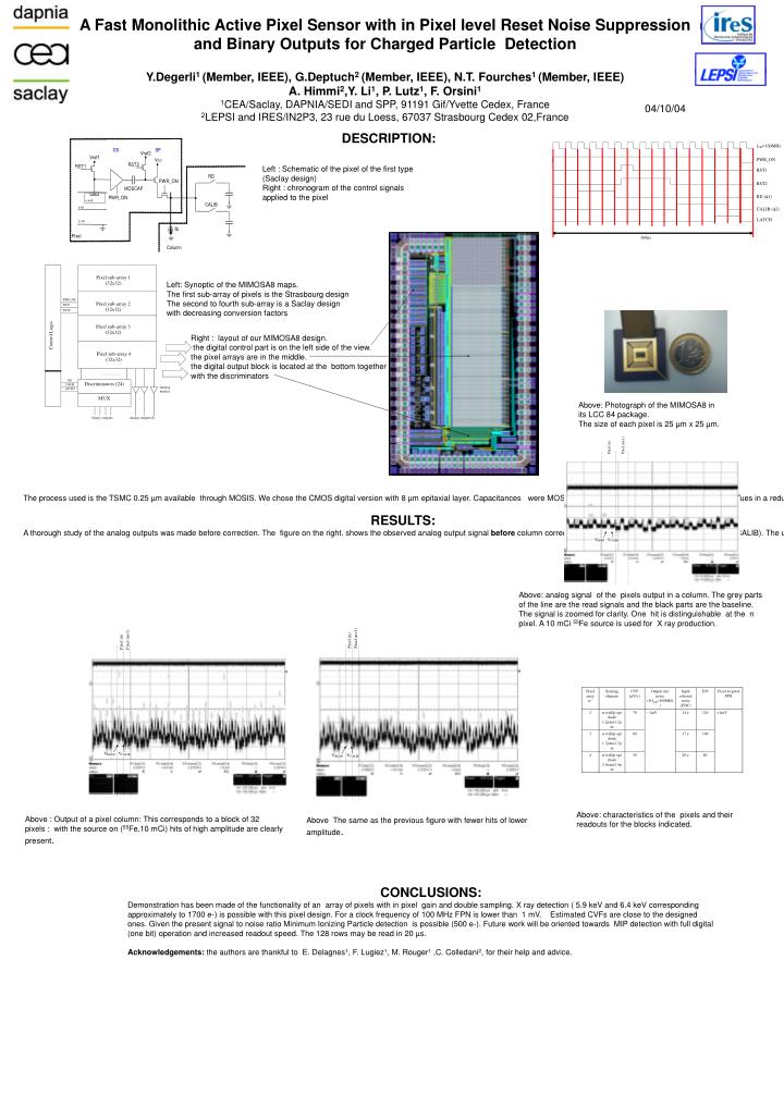
04/10/04. DESCRIPTION:. Left : Schematic of the pixel of the first type (Saclay design) Right : chronogram of the control signals applied to the pixel.

E N D
04/10/04 DESCRIPTION: Left : Schematic of the pixel of the first type (Saclay design) Right : chronogram of the control signals applied to the pixel A Fast Monolithic Active Pixel Sensor with in Pixel level Reset Noise Suppression and Binary Outputs for Charged Particle DetectionY.Degerli1 (Member, IEEE), G.Deptuch2 (Member, IEEE), N.T. Fourches1 (Member, IEEE)A. Himmi2,Y. Li1, P. Lutz1, F. Orsini11CEA/Saclay, DAPNIA/SEDI and SPP, 91191 Gif/Yvette Cedex, France2LEPSI and IRES/IN2P3, 23 rue du Loess, 67037 Strasbourg Cedex 02,France Left: Synoptic of the MIMOSA8 maps. The first sub-array of pixels is the Strasbourg design The second to fourth sub-array is a Saclay design with decreasing conversion factors Right : layout of our MIMOSA8 design. the digital control part is on the left side of the view. the pixel arrays are in the middle. the digital output block is located at the bottom together with the discriminators Above: Photograph of the MIMOSA8 in its LCC 84 package. The size of each pixel is 25 µm x 25 µm. The process used is the TSMC 0.25 µm available through MOSIS. We chose the CMOS digital version with 8 µm epitaxial layer. Capacitances were MOS structures whose advantage is to provide high values in a reduced area. The discriminators are of the same design as the one used for MIMOSA6 (Y. Degerli et al. “Low-power autozeroed high speed comparator for the readout chain of a CMOS monolithic active pixel sensor based vertex detector”, IEEE Transactions on Nuclear Science, vol. 50, no. 5, October 2003,pp 1709-1717). The pixel were designed in order to obtain different conversion factors (CVFs) by adjusting the gain at the sensitive node of the pixel. RESULTS: A thorough study of the analog outputs was made before correction. The figure on the right. shows the observed analog output signal before column correction. Note the 2 levels for each pixel (VRD and VCALIB). The useful signal is the difference between these two levels. Tests without the source show that double sampling eliminates offset dispersions of the in-pixel amplifying stage. The offset dispersions of the output stage is corrected later by the column readout circuitry (discriminators). The functionality of the digital output was also proved here. The typical consumption of each pixel is reduced to 40 µA. Above: analog signal of the pixels output in a column. The grey parts of the line are the read signals and the black parts are the baseline. The signal is zoomed for clarity. One hit is distinguishable at the n pixel. A 10 mCi 55Fe source is used for X ray production. Above: characteristics of the pixels and their readouts for the blocks indicated. Above : Output of a pixel column: This corresponds to a block of 32 pixels : with the source on (55Fe,10 mCi) hits of high amplitude are clearly present. Above The same as the previous figure with fewer hits of lower amplitude. CONCLUSIONS: Demonstration has been made of the functionality of an array of pixels with in pixel gain and double sampling. X ray detection ( 5.9 keV and 6.4 keV corresponding approximately to 1700 e-) is possible with this pixel design. For a clock frequency of 100 MHz FPN is lower than 1 mV. Estimated CVFs are close to the designed ones. Given the present signal to noise ratio Minimum Ionizing Particle detection is possible (500 e-). Future work will be oriented towards MIP detection with full digital (one bit) operation and increased readout speed. The 128 rows may be read in 20 µs. Acknowledgements: the authors are thankful to E. Delagnes1, F. Lugiez1, M. Rouger1 ,C. Colledani2, for their help and advice.