Download
1 / 19
190 likes | 361 Views
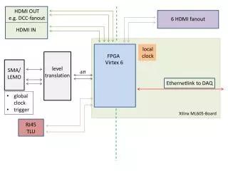
RXP FPGA B. Carlson. EVLA Correlator F2F Meeting Dec. 11-12, 2007. Outline. Testing/schedule described in last talk…so: Overview of functionality; signal integrity (S.I.). Design status. Risks. Functionality. Re-times signals from X-bar Boards in Station racks.

E N D
RXP FPGAB. Carlson EVLA Correlator F2F Meeting Dec. 11-12, 2007
Outline • Testing/schedule described in last talk…so: • Overview of functionality; signal integrity (S.I.). • Design status. • Risks. EVLA Correlator F2F Meeting - RXP FPGA
Functionality • Re-times signals from X-bar Boards in Station racks. • 2 required on each Baseline Board. • Each receives 16 wafers…each wafer is 1 sub-band pair from one station. • 160 lines (+52 spares) connecting chips, operating at 512 Mbps DDR allows each chip to have access to all 32 wafers. • Each chip contains a 32 x 16 full cross-bar switch. • Required for sub-arraying flexibility. • Each chip can phase (at least) 1 stream, all stations. • Multiple outputs for VLBI, auto-corr, auxiliary use. EVLA Correlator F2F Meeting - RXP FPGA
1:2 LVDS buf at Y recirc Rx. EVLA Correlator F2F Meeting - RXP FPGA
1:2 LVDS buf at X recirc Rx. EVLA Correlator F2F Meeting - RXP FPGA
512 Mbps DDR, 1.8 V waveform EVLA Correlator F2F Meeting - RXP FPGA
512 Mbps DDR, 1.8 V eye EVLA Correlator F2F Meeting - RXP FPGA
Yeah, but X-talk is likely to dominate S.I. • However: can arrange for all signals on same layer or not separated by GND planes to switch at the same time to minimize effects of X-talk (haven’t done…can do if problem). EVLA Correlator F2F Meeting - RXP FPGA
RXP-to-GigE FPGA LVDS, at GigE Rx Rx eye EVLA Correlator F2F Meeting - RXP FPGA
Design Status • Critical receive/sync/x-bar/transmit functions implemented and RTL tested…currently running gate-level sims. • Phasing logic planned, still to be implemented. Full RFS/register set defined; GUI layout defined. • Ready for Baseline Board proto arrival in Jan/08. EVLA Correlator F2F Meeting - RXP FPGA
Risks • # LVDS receiver/transmitters…never been tested before. • 512 Mbps DDR: analysis/sim/functionality…looks good, but never been tested before. • Phasing won’t fit into one chip? • Using big EP2S60 device…w/o phasing ~40% logic use. • Can split into 2 chips or even 3 chips if necessary. EVLA Correlator F2F Meeting - RXP FPGA
Summary • Overview of functionality. • Design status; S.I. • Risks. EVLA Correlator F2F Meeting - RXP FPGA