Download
1 / 14
180 likes | 404 Views
The Fate of Silicon Technology: Silicon Transistors. Maria Bucukovska Scott Crawford Everett Comfort. The Silicon Transistor. Metal-oxide-semiconductor (MOS) transistor Used primarily as a switch in digital devices Has 3 electrodes: source, gate and drain

E N D
The Fate of Silicon Technology:Silicon Transistors Maria Bucukovska Scott Crawford Everett Comfort
The Silicon Transistor • Metal-oxide-semiconductor (MOS) transistor • Used primarily as a switch in digital devices • Has 3 electrodes: source, gate and drain • Consists of semiconductor substrate: silicon • Gate Oxide: separates Silicon form the electrodes www.mse.cornell.edu/ courses/engri111/transist.htm
How It Works • Electron flow between source and drain is controlled by altering the gate voltage • This allows Si to act either as a conductor or an insulator • Therefore, the transistor can store an on/off signal • If the voltage at the gate electrode is "on" the transistor is also "on", and current flow between the source and drain electrodes is possible with negligible losses. • If the voltage at the gate electrode is "off", the transistor is also "off", and no current flows between the source and drain electrode.
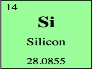
Silicon • Superiority of Silicon over other semiconductors due to its oxide • Silicon dioxide : • Has good insulating properties • Can be removed easily, greatly simplifying the fabrication of integrated circuits
History of the Silicon Transistor (1950’s-1970’s) • 1950’s: Si emerged as choice material for transistors • 1958-59: transistors began being mass produced; many transistors could be interconnected on a Si surface using photolithography • 1960: First MOS transistor developed • 1971: Intel fabricated its first transistor-based single-chip microprocessor: the four-bit “Intel 4004” • Size of the MOS transistor was 10 μm • 2300 transistors integrated onto the Intel chip
Moore's Law • Gordon Moore of Intel predicted a trend in the density of microchips (heavily based on transistor size) • Predicted that the number of components that could be crammed into an integrated circuit would double every 2 years for the near future • Highly based on transistors and reducing the gate length • His theory should continue for the next two decades, but after that, the manufacturing techniques of Silicon used today will no longer be possible to sustain the exponential trend • Moore’s law is coming to an end due to fundamental physical limitations • Challenge: Find a way to connect nano-scale transistors to make giga-scale circuits
Today • Overall, the transistor has evolved in 2 ways: • Has become much smaller; most modern devices measure a thousandth of the original size • The number of transistors that can be interconnected on a single chip has increased from a few tens to hundreds of millions • The advance in microelectronics is heavily based on • reducing the gate length,which is the distance between • the source and drain contacts • Today, transistors have gate lengths of less than 50 nm • Presently, the latest Intel microprocessor uses more than half a billion • transistors on a single chip, each one is 45 nm in size, squeezed onto • single chip of area 3cm2 • 4 Gb chips are in production today • 16 Gb chips are being developed currently, which will contain • 160 billion transistors
Today’s Predictions: • Every 6 years, the gate length of the MOS transistor will be halved: 37 nm in 2004, 18nm in 2010, and 9 nm by 2016 • In accordance with Moore’s Law, the number of transistors on a chip will continue doubling every 2 years up to 20 years • Single-electron transistors based on quantum dots are in existence today (1 nm in size), but they are difficult to make and even harder to connect in large numbers • Soon we will start to develop quantum devices that operate on spin rather than electron charge-transistors could be smaller than 1 nm in size
Future Obstacles and Possible Solutions • Building a transistor with a gate length less than 10 nm: • Obstacle = gate oxide must have large enough capacitance to allow for proper control of current • To overcome this challenge, the thickness of the oxide must be reduced from 1.2 nm to 0.7 nm, reducing the gate length • This means using just 2 atomic layers, which is the ultimate manufacturing limit of bulk silicon oxide • Alternative option to avoid this limit: use substance with higher dielectric constant than silicon oxide- • Ex-hafnium-oxide film can have the same capacitance as silicon oxide, but it can be up to five times thicker
Another obstacle: the short-channel effect • In ultra short channels, electron tunneling from the source to the drain occurs (even when transistor is off) • This results in a large leakage current which is usually suppressed by increasing the doping concentration in the channel region • However, when utilizing devices smaller than 100 nm in size, increased doping results in decreased channel mobility • This decreases the performance of the transistor
Possible Solution: the double-gate MOS field effect transistor • Geometry of double-gate allows more control over electrostatic potential of the channel, meaning short-channel effects can be reduced • Therefore, there will be a lowered degree of channel doping , and consequently shorter gate lengths can be achieved VS. Normal MOS transistor Double-gate MOS transistor “Silicon Microelectronics.” Physics World. September 2005
Speed is also a factor in addition to size, in effective silicon transistors • “Strained silicon” is a stretched lattice of silicon that allows faster electron flow with less resistance. Therefore faster transistors. • Intel is developing a tri-gate transistor to improve similar-sized transistors but with 3 times the active transistor area. Current flows along the top face and side walls of the transistor. http://www.intel.com/technology/silicon/si10031.htm
Our Conclusions • Despite the effectiveness of the silicon transistor in nanotechnologies it seems as though the room for improvement grows slim as the limitations of the perhaps outdated material become more prevalent. Future technologies may require different materials to continue the “shrinking” trend of transistors, whether it means adding new materials with silicon technologies or replacing them indefinitely.