Download
1 / 32
320 likes | 483 Views
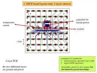
+44 (0)1992 510000. Manufacturing Processes for a 4 Layer Multi-layer PCB. Tracks under solder mask. The following presentation covers the main processes during the production of a 4 layer or a multi-layer PCB. The diagrams which follow represent a section through a PCB, as indicated

E N D
+44 (0)1992 510000 Manufacturing Processes for a 4 Layer Multi-layer PCB Tracks under solder mask The following presentation covers the main processes during the production of a 4 layer or a multi-layer PCB. The diagrams which follow represent a section through a PCB, as indicated in red. Via hole SMD Pad Section through PCB
+44 (0)1992 510000 Typical Layer Construction - 4 Layer PCB Copper Laminate COPPER FOIL Layer 1 (Outer) PRE-PREG Layer 2 (Inner) INNER LAYER (CORE) 4 Layer PCB’s Layer 3 (Inner) PRE-PREG • Multilayer PCB’s have inner tracking layers which are individually processed layer pairs which require bonding and connecting to form the finished PCB. COPPER FOIL Layer 4 (Outer)
+44 (0)1992 510000 Inner Layer Processing Copper Laminate (Dielectric) Layer 2 (Inner) • For Multilayer PCB’s Inner layer Core materials are usually processed as “Layer pairs” • Core materials can be typically 0.2mm thick which come pre coated with a ½ oz copper foil. Core Layer 3 (Inner)
+44 (0)1992 510000 Laminating and Imaging of Internal Layers UV sensitive film is laminated over top and bottom surfaces of the Core Areas of the Core where no copper is required are left exposed Inner Layer Imaging Layer 2 (Inner) • The addition of the inner layer track patterns to layers 2 and 3. Core Layer 3 (Inner)
+44 (0)1992 510000 Etch Process - Remove Exposed Copper Copper Removed Inner Layer Etching Layer 2 (Inner) • The etch process produces an ‘etch back’ or undercut of the tracks. This can be specified by the W / W1 parameters • This means that tracks will end up approximately • 0,025 mm (0.001”) thinner than the original design. Core Layer 3 (Inner)
+44 (0)1992 510000 Remove Laminating Film Film Strip Layer 2 (Inner) • The laminated film is removed prior to AOI inspection. Core Layer 3 (Inner)
+44 (0)1992 510000 Completed Inner Layer Core All inner layer Core materials are processed as “Layer Pairs” prior to Bonding At this stage the Cores are inspected visually (AOI) and defective Cores rejected Sometimes a surface treatment is applied to the Cores to aid with the Bonding process AOI Inspection Layer 2 (Inner) • Automatic Optical Inspection (AOI). • Inner layers are scanned and compared to Gerber data for errors. Core Layer 3 (Inner)
+44 (0)1992 510000 Layer stackup FOIL Layer 1 (Outer) PRE-PREG Layer 2 (Inner) INNER LAYER Layer 3 (Inner) PRE-PREG FOIL Layer 4 (Outer) Layer Stackup • The order in which the layers are to be bonded together. • The outer layer copper foils, layers 1 and 4 are purchased in sheet form. For a 1 oz finished copper weight typically a ½ oz foil would be used during bonding process to form the outer layers. Layer 1 (Outer) FOIL Layer 2 (Inner) PRE-PREG Layer 3 (Inner) INNER LAYER PRE-PREG Layer 4 (Outer) FOIL
+44 (0)1992 510000 Layer stackup FOIL Layer 1 (Outer) PRE-PREG Layer 2 (Inner) INNER LAYER Layer 3 (Inner) PRE-PREG FOIL Layer 4 (Outer) Layer 1 (Outer) FOIL Layer 2 (Inner) PRE-PREG Layer 3 (Inner) INNER LAYER PRE-PREG Layer 4 (Outer) FOIL
+44 (0)1992 510000 Layer stackup FOIL Layer 1 (Outer) PRE-PREG Layer 2 (Inner) INNER LAYER Layer 3 (Inner) PRE-PREG FOIL Layer 4 (Outer) Layer 1 (Outer) FOIL Layer 2 (Inner) PRE-PREG Layer 3 (Inner) INNER LAYER PRE-PREG Layer 4 (Outer) FOIL
+44 (0)1992 510000 Layer stackup FOIL Layer 1 (Outer) PRE-PREG Layer 2 (Inner) INNER LAYER Layer 3 (Inner) PRE-PREG FOIL Layer 4 (Outer) Layer 1 (Outer) FOIL Layer 2 (Inner) PRE-PREG Layer 3 (Inner) INNER LAYER PRE-PREG Layer 4 (Outer) FOIL
+44 (0)1992 510000 Layer stackup FOIL Layer 1 (Outer) PRE-PREG Layer 2 (Inner) INNER LAYER Layer 3 (Inner) PRE-PREG FOIL Layer 4 (Outer) Layer 1 (Outer) FOIL Layer 2 (Inner) PRE-PREG Layer 3 (Inner) INNER LAYER PRE-PREG Layer 4 (Outer) FOIL
+44 (0)1992 510000 Layer stackup FOIL Layer 1 (Outer) PRE-PREG Layer 2 (Inner) Layer 3 (Inner) PRE-PREG FOIL Layer 4 (Outer) Layer 1 (Outer) FOIL Layer 2 (Inner) PRE-PREG Layer 3 (Inner) INNER LAYER PRE-PREG Layer 4 (Outer) FOIL
+44 (0)1992 510000 Layer stackup FOIL Layer 1 (Outer) PRE-PREG Layer 2 (Inner) Layer 3 (Inner) PRE-PREG FOIL Layer 4 (Outer) Layer 1 (Outer) FOIL Layer 2 (Inner) PRE-PREG Layer 3 (Inner) INNER LAYER PRE-PREG Layer 4 (Outer) FOIL
+44 (0)1992 510000 Layer stackup FOIL Layer 1 (Outer) PRE-PREG Layer 2 (Inner) Layer 3 (Inner) PRE-PREG FOIL Layer 4 (Outer) Layer 1 (Outer) FOIL Layer 2 (Inner) PRE-PREG Layer 3 (Inner) INNER LAYER PRE-PREG Layer 4 (Outer) FOIL
+44 (0)1992 510000 Bonding – Heat FOIL Layer 1 (Outer) PRE-PREG Layer 2 (Inner) Layer 3 (Inner) PRE-PREG FOIL Layer 4 (Outer) Bonding • Once the layers are built up heat is applied over a period of time, this is to allow the Pre-Preg material time to melt and flow evenly between the layers, this is in effect the material that sticks the layers together. Layer 1 (Outer) FOIL Layer 2 (Inner) PRE-PREG Layer 3 (Inner) INNER LAYER PRE-PREG Layer 4 (Outer) FOIL
+44 (0)1992 510000 Bonding – Multilayer Press FOIL Layer 1 (Outer) PRE-PREG Layer 2 (Inner) Layer 3 (Inner) PRE-PREG FOIL Layer 4 (Outer) Bonding • Layers are pressed together over a set period of time typically a bonding cycle will last for approx. 4 hours. • Bonding capacity would depend on the number of openings and size of press.
+44 (0)1992 510000 Drilling of a Panel Drilled Hole Copper Laminate Layer 1 Drilling • The holes are drilled for both thru-hole components and via connections. Once plated this will form the connection from 1 side of the PCB to the other, at the same time connecting the inner layers where required. Layer 4
+44 (0)1992 510000 Electroless Copper Process Addition of Copper to all Exposed Surfaces Drilled Hole Copper Layer 1 Plating Layer 2 • Plating is the same process for 2 or 4 Layer. • The aim is plate down the barrel of the hole to make the connection from 1 side of the PCB to the other. Layer 3 Layer 4
+44 (0)1992 510000 Laminating and Imaging of External Layers UV sensitive film is laminated over top and bottom surfaces of PCB It is then exposed and developed, leaving an exposed image of the PCB pattern Layer 1 Imaging Layer 2 • The outer layer track patterns are photo-imaged onto the panels using UV sensitive film. Layer 3 Layer 4 Copper
+44 (0)1992 510000 Electro-plating Process 1 Additional Copper to all Exposed Surfaces Laminated Film Plate Additional Copper Layer 1 Plating Layer 2 • Electro-plating increases the copper thickness on the outer layers and through the barrel of the hole. The copper foils for a 4 layer or the starting copper weight on 2 layer boards is most commonly ½ oz the plating then increases the finished copper weight to the desired 1oz each side. Layer 3 Layer 4
+44 (0)1992 510000 Electro-plating Process 2 Add Tin over Exposed Copper Areas Tin Plating Laminated Film Additional Copper Layer 1 Tin Plating Layer 2 • A tin plate is added to all exposed copper areas, this act as a mask during the etching process. Layer 3 Layer 4
+44 (0)1992 510000 Electro-plating Process 3 Remove Laminated Film Tin Plating Laminated Film Removed Layer 1 Film Strip Layer 2 • The laminated film is removed to expose copper areas ready for the etching process. Layer 3 Layer 4
+44 (0)1992 510000 Etch Process - Remove Exposed Copper Tin Plating Copper Removed Layer 1 Etching Process Layer 2 • The etching process removes unwanted areas of copper. • The etch process produces an ‘etch back’ or undercut of the tracks. • This means that tracks will end up approximately • 0,025 mm (0.001”) thinner than the original design. Layer 3 Layer 4
+44 (0)1992 510000 Tin Strip - Remove Tin Plating Tin Plating Removed Layer 1 Tin Strip Layer 2 • The Removal of Tin will very slightly reduce the copper thickness (T) on the outer layers Layer 3 Layer 4
+44 (0)1992 510000 PCB is now complete except for surface finishes and panel routing/punching Via Hole SMD Pad Tracks Layer 1 Layer 4 Tracks
+44 (0)1992 510000 Solder Mask Application Image, Develop and Cure UV Image, Develop and Cure Layer 1 Solder Mask • The image is semi cured and then UV image exposed. • Any areas that are not exposed to the UV light are then dissolved in the developer, exposing the areas where the final surface finish is required. Layer 4
+44 (0)1992 510000 Surface Finish Process Apply Solder to Exposed Copper Areas Layer 1 Surface Finish • Surface Finish (Tin / Lead, Gold, Silver, OSP, Tin) is usually only added to pads. The solder mask prevents coating of any other areas. Layer 4
+44 (0)1992 510000 Component Ident SCL2 9624 Ident / Silk Screen • An optional component Ident or Silk Screen is printed onto the PCB.
+44 (0)1992 510000 Routing or Punching Routing or Punching • The circuit profile is then punched or routed.
+44 (0)1992 510000 Testing and Inspection All PCB’s are 100% Electrically tested All PCB’s are 100% Visually Inspected