Download
1 / 1
80 likes | 479 Views
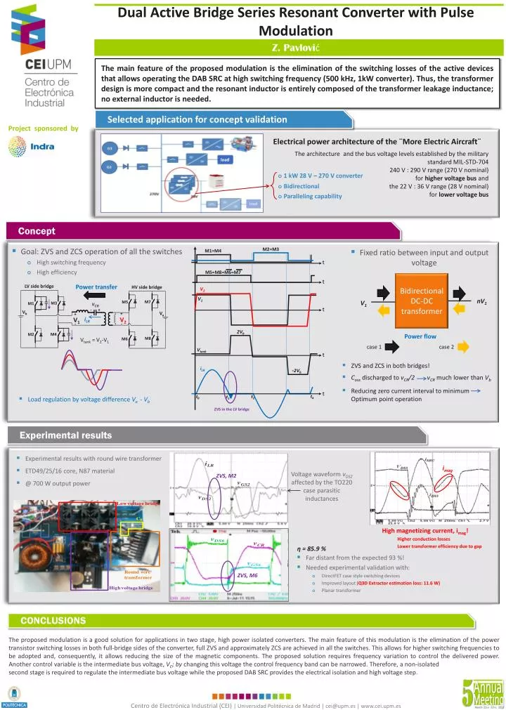
M2=M3. Dual Active Bridge Series Resonant Converter with Pulse Modulation. M1=M4. Z. Pavlovi ć. M5=M8=M6=M7. loa d.

E N D
M2=M3 Dual Active Bridge Series ResonantConverterwith Pulse Modulation M1=M4 Z. Pavlović M5=M8=M6=M7 load The main feature of the proposed modulation is the elimination of the switching losses of the active devices that allows operating the DAB SRC at high switching frequency (500 kHz, 1kW converter). Thus, the transformer design is more compact and the resonant inductor is entirely composed of the transformer leakage inductance; no external inductor is needed. V2 Vtank V1 Selected application for concept validation Project sponsored by Electrical power architecture of the ¨More Electric Aircraft¨ The architecture and the bus voltage levels established by the military standard MIL-STD-704 240 V : 290 V range (270 V nominal)for higher voltage busand the 22 V : 36 V range (28 V nominal)for lowervoltage bus iLR • 1 kW 28 V – 270 V converter • Bidirectional • Parallelingcapability load Concept • Goal: ZVS and ZCS operation of all the switches • High switching frequency • High efficiency • Fixed ratio between input and output voltage t Bidirectional DC-DC transformer t Power transfer LV side bridge HV side bridge nV1 V1 M7 M5 vCR M3 M1 + - Vb Va + + V2 iLR V1 t - - M4 M2 Powerflow M8 M6 Vtank = V2-V1 2Vb case 1 case 2 • ZVS and ZCS in both bridges! t • CossdischargedtovCR/2 vCRmuchlowerthanVb -2Vb • ReducingzerocurrentintervaltominimumOptimum pointoperation • Load regulationbyvoltagedifferenceVa- Vb t t4 t0 t2 t1 Experimental results • ZVS in the LV bridge • Experimental resultswith round wiretransformer imag • ETD49/25/16 core, N87 material • VoltagewaveformvDS2affectedbythe TO220 case parasiticinductances ZVS, M2 • @ 700 W output power • Highmagnetizingcurrent, imag! • Higherconductionlosses • Lowertransformerefficiencydueto gap η = 85.9 % • Fardistantfromtheexpected 93 %! • Needed experimental validationwith: • DirectFET case style switching devices • Improved layout (Q3D Extractor estimationloss: 11.6 W) • Planar transformer ZVS, M6 CONCLUSIONS The proposed modulation is a good solution for applications in two stage, high power isolated converters. The main feature of this modulation is the elimination of the power transistor switching losses in both full-bridge sides of the converter, full ZVS and approximately ZCS are achieved in all the switches. This allows for higher switching frequencies to be adopted and, consequently, it allows reducing the size of the magnetic components. The proposed solution requires frequency variation to control the delivered power. Another control variable is the intermediate bus voltage, VC; by changing this voltage the control frequency band can be narrowed. Therefore, a non-isolated second stage is required to regulate the intermediate bus voltage while the proposed DAB SRC provides the electrical isolation and high voltage step.