Download
1 / 25
320 likes | 836 Views
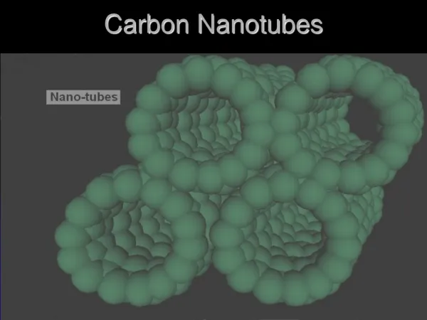
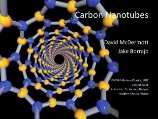
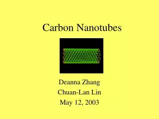
Carbon Nanotubes. CARBON NANOTUBES. Discovered in 1991 by Sumiyo Iijima , a Japanese scientist working at the NEC Corporation. Is a tubular form of carbon with a diameter as small as 0.4 nm and length from a few nanometers up to a millimeter.

E N D
CARBON NANOTUBES • Discovered in 1991 by SumiyoIijima, a Japanese scientist working at the NEC Corporation. • Is a tubular form of carbon with a diameter as small as 0.4 nm and length from a few nanometers up to a millimeter. • Length-to-diameter ratio of a carbon nanotube can be as large as 28,000,000:1, which is unequalled by any other material. • Carbon exists in several forms; graphite and diamond are the most familiar. • A CNT is characterized by its Chiral Vector: Ch = n â1 + m â2,
Formation of CNT • Process which is used to form these Nanotubes, is called Chemical Vapor Deposition. • Can be made in a standard chemistry laboratory. • A quartz tube about 1 inch in diameter serves as the growth reactor and is inserted inside a tube furnace. Scanning electron microscopy of nanofibers covered with nanotubes
Tube furnace is a standard heating device for conducting, syntheses and purifications. • Nanotube grows on a silicon wafer that is placed at a central location inside the quartz tube. • A thin layer of iron or nickel or cobalt is applied to the silicon wafer to serve as a catalyst to grow the nanotubes. • In a few minutes, the silicon wafer appears black, indicating that it is covered with nanotubes.
Types of CNTs • Single Wall CNT (SWCNT) • Multiple Wall CNT (MWCNT) Can be metallic or semiconducting depending on their geometry.
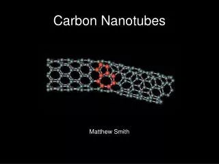
Single Walled CNT’s • Made by a single layer of a graphite sheet, cutting it into a small piece of any size, and rolling it. Single-walled carbon nanotubes
SWCNT…. • Characterized by a set of two integers (n, m) called the Chirality vector. • When (n-m)/3 is an integer (for example when n is 8 and m is 2), then the nanotube has metallic properties. • If (n-m)/3 is not an integer, the corresponding nanotube behaves like it is a semiconductor. • Ability to create tubes of either metallic or semiconductor nature is of great practical importance.
Conti.. • Single wall carbon nanotubes exhibit extraordinary mechanical properties. • Hundred times stronger than steel at one-sixth of its weight. • Ability to carry current and heat along the axial direction is extraordinary. • Has the potential to replace copper wires as conductors. • Scientists and engineers envision all carbon-based electronics using semiconducting and metallic carbon nanotubes of different values of n and m.
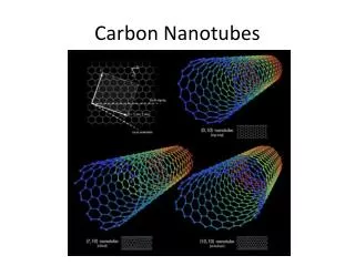
Types of Single-Walled Carbon Nanotubes n and m can be counted at the end of the tube Zigzag (n,0)
Types of Single-Walled Carbon Nanotubes Armchair (n,n) Chiral (n,m)
Armchair (n,m) = (5,5) = 30 ZigZag (n,m) = (9,0) = 0 Chiral (n,m) = (10,5) 0 < < 30
MWCNT A tower of multiwalled carbon Nanotubes
Take multiple layers of a graphite sheet and roll them in the form of a cylinder.
Fig. 2. (a). Band structure of a graphene sheet (top) and the first Brillouin zone (bottom). (b) Band structure of a metallic (3,3) CNT. (c) Band structure of a (4,2) semiconducting CNT. The allowed states in the nanotubes are cuts of the graphene bands indicated by the white lines. If the cut passes through a K point, the CNT is metallic; otherwise, the CNT is semiconducting.
Nanotubes Growth Methods a) Arc Discharge b) Laser Abalation • Involves condensation of C-atoms generated from evaporation of solid carbon sources. Temperature ~ 3000-4000K, close to melting point of graphite. • Both produce high-quality SWNTs and MWNTs. • MWNT: 10’s of m long, very straight & have 5-30nm diameter. • SWNT: needs metal catalyst (Ni,Co etc.). Produced in form of ropes consisting of 10’s of individual nanotubes close packed in hexagonal crystals.
Nanotubes Growth Methods c) Chemical Vapor Deposition: Hydrocarbon + Fe/Co/Ni catalyst 550-750°C CNT Steps: • Dissociation of hydrocarbon. • Dissolution and saturation of C atoms in metal nanoparticle. • Precipitation of Carbon. Choice of catalyst material? Base Growth Mode or Tip Growth Mode? • Metal support interactions
Application Electrical • Field emission in vacuum electronics • Building block for next generation of VLSI • Nano lithography Energy storage • Lithium batteries • Hydrogen storage Biological • Bio-sensors • Functional AFM tips • DNA sequencing
Challenges & Future.. Future applications: • Already in product: CNT tipped AFM • Big hit: CNT field effect transistors based nano electronics. • Futuristic: CNT based OLED, artificial muscles… Challenges: • Manufacture: Important parameters are hard to control. • Large quantity fabrication process still missing. • Manipulation of nanotubes.
Conclusion • Their phenomenal mechanical properties, and unique electronic properties make them both interesting as well as potentially useful in future technologies. • Significant improvement over current state of electronics can be achieved if controllable growth is achieved. • Growth conditions play a significant role in deciding the electronic and mechanical properties of CNTs. • Growth Mechanisms yet to be fully established.