Download
1 / 11
110 likes | 120 Views
Radiation Damage Studies for Solid State Sensors Subject to MRaD Doses [T506 2015 Report]. Bruce Schumm UC Santa Cruz August 5 2015. T506 Purpose/Goals. Purpose is to explore the radiation hardness and annealing properties of sensor candidates for the ILC BeamCal

E N D
Radiation Damage Studies for Solid State Sensors Subject to MRaD Doses [T506 2015 Report] Bruce Schumm UC Santa Cruz August 5 2015
T506 Purpose/Goals Purpose is to explore the radiation hardness and annealing properties of sensor candidates for the ILC BeamCal BeamCal expected to receive ~100MRad/yr of electromagnetically-induced radiation Sensor types include four Si-diode technologies, GaAs, Sapphire and SiC Prior running suggest Si-diode detectors may be robust in terms of charge collection but currents may be high. GaAs charge collection noticeably affected at ~5 MRad 2
Incorporate hadronic processes by placing sensor at maximum of tungsten-induced shower Up to 10W beam absorption; operate at about freezing to avoid annealing 3
Actual Setup In ESA Beamline 2 X0 pre-radiator; introduces a little divergence in shower Sensor sample Not shown: 4 X0 and 8 X0 radiators just before and after sensor
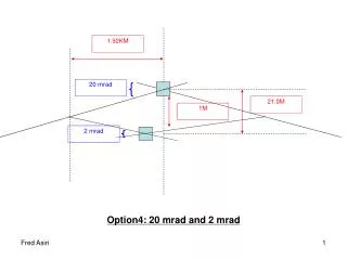
Proposed split radiator configuration 5mm Tungsten “pre” 13mm Tungsten “post” Separated by 1m Fluence (particles per cm2) 1.0 2.0 3.0 5 Radius (cm)
Rastering Need uniform illumination over 0.25x0.75 cmregion (active area of SCIPP’s charge collection measurement apparatus). • Raster in 0.05cm steps over 1x1 cm, assuming fluence profile on prior slide (see next slide for result)
Exposure Rate at 13.32 GeV Use simulation, verified in first run with RadFET measurement, to calculate “shower conversion factor” (averaged over rastering pattern) (Ebeam) = (fluence)/(incident electron) (13.32) = 33.5 (e/cm2)/(incident electron) Dose = * Q(nC) * 160 (rad-cm2/nC) At 1.02x10⁹ e-/pulse, dose is 874 rad/pulse. At 5 Hz 4.37 krad/s 15.7 Mrad/Hr
T506 Ambitions 15 Mrad/hr 200 Mrad in 20 hours (2 shifts) Goal: • 300 Mrad exposure of P-type Si diode (2 shifts) • 300 Mrad exposure of N-type Si diode (2 shifts) • 100 Mrad exposure of new SiC sensor (1 shift)
T506 Actuals July 31 – Aug 1: • PPS problem, setup no dose accumulated Aug 1-2: • 9 hours running, 135 Mrad on P-type diode Aug 2-3: • Actuator and camera issues; no dose Aug 3-4: • 9 hours running, total of 273 Mrad on P-type • Dedicated (no radiator) run confirms alignment Aug 4-5: • Accumulate 100 Mrad on SiC in ~6 hrs • LCLS-II ceramic capacitor damage study (Beukers)
T506 Summary • Alignment and transport estasblished with dedicated beam time • 270 Mrad exposure of P-type Si diode sensor (T506 record!) • 100 Mrad exposure of SiC sensor (new type of sensor) • LCLS-II radiation damage study performed Successful run! Many thanks to all…