Download
1 / 46
470 likes | 496 Views
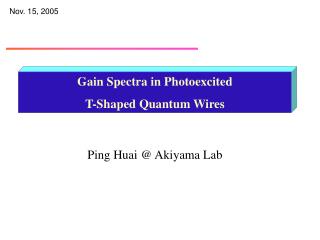
2004 Fall MRS meeting in Boston (2004.11.30 B3.1). T-shaped quantum-wire laser. M. Yoshita, Y. Hayamizu, Y. Takahashi, H. Itoh, T. Ihara, and H. Akiyama Institute for Solid State Physics, Univ. of Tokyo and CREST, JST. L. N. Pfeiffer , K. W. West, and Ibo Matthews

E N D
2004 Fall MRS meeting in Boston (2004.11.30 B3.1) T-shaped quantum-wire laser M. Yoshita, Y. Hayamizu, Y. Takahashi, H. Itoh, T. Ihara, and H. Akiyama Institute for Solid State Physics, Univ. of Tokyo and CREST, JST L. N. Pfeiffer, K. W. West, and Ibo Matthews Bell Laboratories, Lucent Technologies 1. Formation of high-quality GaAs T-shaped quantum wires Cleaved-edge overgrowth with MBE, AFM, PL, PLE 2. Single-wire laser PL scan, Lasing, PL, Absorption/Gain via Cassidy’s method, Transmission 3. Observation of RT 1D exciton absorption in 20-wire laser 4. Optical response of n-doped single-wire FET device
GaAs substrate Cleaved-edge overgrowth with MBE by L. N. Pfeiffer et al., APL 56, 1679 (1990). [110] [001] Cleave in situ (001) MBE Growth (110) MBE Growth 600oC 490oC (490oC)
Good Poor Bad Nomarski Microscope Images of Cleaved-Edge- Overgrowth Surfaces “Hackling”
High Quality 490C Growth T-wire ??? Atomically flat interfaces (By Yoshita et al. JJAP 2001)
High Quality 490C Growth 510-600C Anneal T-wire !? Atomically flat interfaces (By Yoshita et al. JJAP 2001)
High Quality 490C Growth 510-600C Anneal T-wire !!? Atomically flat interfaces (By Yoshita et al. JJAP 2001)
High Quality 490C Growth 510-600C Anneal T-wire !!!!! Atomically flat interfaces (By Yoshita et al. JJAP 2001)
20-wire laser sample 14nm x 6nm 1st growth 600C 2nd growth 490C (arm well) 600C 10min anneal 490C (cover layers) Laser bars 500mm uncoated cavity
PL and PLE spectra Sharp PL width Small Stokes shift 1D free exciton 1D continuum states arm well T-wire stem well (Akiyama et al. APL 2003)
E-field E-field // to wire _ to wire // to arm well I
Single quantum wire laser Probability of Photon Cavity length500 mm G=5x10⁻⁴ Probability of Electron
Scanning micro-PL spectra scan T-wire stem well T-wire stem well T=5K ContinuousPL peak over 20 mm PL width < 1.3 meV
Lasing in a single quantum wire 500mm gold-coated cavity Threshold 5mW (Hayamizu et al, APL 2002)
Excitation power dependence of PL M. Yoshita, et al.
n1D = 1.2 x 106 cm-1 (rs = 0.65 aB) aB ~13nm Electron-hole Plasma Density n1D = 1.2 x 105 cm-1 (rs = 6.6 aB) Biexciton+Exciton EB =2.8meV n1D = 3.6 x 103 cm-1 (rs = 220 aB) Free Exciton n1D ~ 102 cm-1
Absorption/gain measurement based on Hakki-Paoli-Cassidy’s analysis of Fabry-Perot-laser emission below threshold :Absorption coeff. :Reflectivity D. T. Cassidy JAP. 56 3096 (1984) Free Spectral Range B. W. Hakki and T. L. Paoli JAP. 46 1299 (1974)
Absorption Spectrum by Cassidy method Cassidy’s Method Single wire laser, uncoated cavity mirrors Excitation Light :cw TiS laser at 1.631eV Spectrometer with spectral resolution of 0.15 meV Point WaveguideEmission Polarizationparallel toArm well
Measurement of absorption/gain spectrum Excitation Light :cw TiS laser at 1.631eV Spontaneousemission Spectrometer with spectral resolution of 0.15 meV Stripe shape Cassidy’s Method WaveguideEmission 8.3mW Polarizationparallel toArm well
Absorption/gain spectrum (High excitation power) Electron-Hole Plasma Absorption Gain EBE EFE 8.3mW Hayamizu et al.
Electron-Hole Plasma • Exciton peak and continuum onset decay without shift. • Gap between exciton and continuum is gradually filled. • Exciton changes to Fermi edge Exciton Hayamizu et al.
Transmittance for single Coupling efficiency = 20% Takahashi et al. unpublished
Absorption for single Takahashi et al. unpublished
Absorption for 20 Y. Takahashi et al.
Absorption at 300 K Room-Temperature 1D Exciton Absorption! Y. Takahashi et al.
e h e e h 14nmx6nm Doped Single Wire FET device with tunable 1D electron density 1D electron density T. Ihara et al.
Summary • GaAs T-shaped quantum wires (T-wires) are formed by cleaved-edge overgrowth with MBE. • Growth-interrupt anneals dramatically improve T-wire quality. • AFM : No atomic steps over 100mm. • PL : Sharp PL width (~1meV) improved by a factor of 10. • PLE : Observation of 1D free exciton, & 1D continuum states • Single wire lasing : The world thinnest laser (14nm x 6nm), • 5mW threshold optical pumping power at 5K. • Gain/absorption measurement by Hakki-Paoli-Cassidy’s method. • Strong photo-absorption by a single wire • 84/cm (98.5% absorption / 500mm) at exciton peak at 5K • Room-temperature exciton absorption observed in 20-wire laser. • Single-wire FET: carrier-sensitive optical responses.
(001) and (110) surfaces of GaAs (110) (001) [001] [110] [110] [001]
Growth rate of GaAs in MBE Substrate rotation >>> uniform holder Substrate Ga limited growth under As4overpressure As Ga
600oC Anneal Atomically flat interfaces (by M. Yoshita et al. JJAP 2001) Interface control by growth-interruption annealing 490oC Growth High Quality T-wire arm well 6nm stem well 14nm
Absorption at higher temperatures by Cassidy Hayamizu et al. unpublished
Evolution of continuum Takahashi et al. unpublished
Lasing & many-body effects in quantum wires E. Kapon et al. (PRL’89) Lasing in excited-states of V-wires W. Wegscheider et al. Lasing in the ground-state of T-wires, no energy shift, (PRL’93) excitonic lasing R. Ambigapathy et al. PL without BGR, strong excitonic effect in V-wires (PRL’97) L. Sirigu et al. (PRB’00) Lasing due to localized excitons in V-wires J. Rubio et al. (SSC’01) Lasing observed with e–h plasma emission in T-wires A. Crottini et al. (SSC’02) PL from exciton molecules (bi-excitons) in V-wires T. Guillet et al. (PRB’03) PL, Mott transition form excitons to a plasma in V-wires H. Akiyama et al. Lasing due to e–h plasma, no exciton lasing in T-wires (PRB’03) F. Rossi and E. Molinari (PRL’96) F. Tassone, C. Piermarocchi, et al. (PRL’99,SSC’99) S. Das Sarma and D. W. Wang (PRL’00,PRB’01) Theories “1D exciton Mott transition”
no energy shift of the exciton band edge • plasma low-energy edges appear at the bi-exciton energy positions, and show BGR • no connection, but coexistence of two band edges no level-crossing between the band edges and the exciton level Physical picture of 1D exciton–plasma transition the exciton Mott transition Our PL results show Increase of e–h pair density causes ・ reduction of exciton binding energy ・ red shift of the band edge (band-gap renormalization (BGR)) eg. D. W. Wang and S. Das Sarma, PRB 64, 195313 (2001). band edge exciton level
Exciton band edge & plasma band edge (T=30K) ▼ plasma band edge (low energy edge of plasma PL) starts at biexciton energy and shows red shift. ▼ exciton band edge, (onset of continuum states) exciton ground and excited states show no shift.
Electron plasma and minority hole e e e e h e e e e e e h e X- Charged Exciton X Exciton e h
Theory 1D exciton and continuum states