Download
1 / 75
820 likes | 1.13k Views
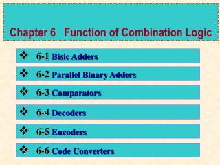
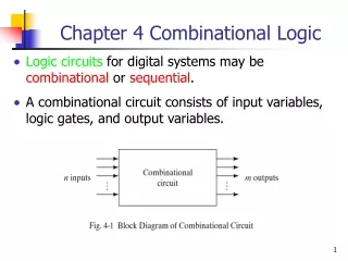
Chapter 4 Combination Logic. 4-1 Combinational Circuits. 4-2 Analysis Procedure. 4-3 Design Procedure. 4-4 Binary Adder-Subtractor. 4-5 Decimal Adder. 4-6 Binary Multiplier. Chapter 4 Combination Logic. 4-7 Magnitude Comparator. 4-8 Decoders. 4-9 Encoders.

E N D
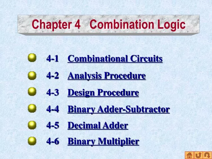
Chapter 4 Combination Logic 4-1 Combinational Circuits 4-2 Analysis Procedure 4-3 Design Procedure 4-4 Binary Adder-Subtractor 4-5 Decimal Adder 4-6 Binary Multiplier
Chapter 4 Combination Logic 4-7 Magnitude Comparator 4-8 Decoders 4-9 Encoders 4-10 Multiplexers 4-11 HDL For Combinational Circuits
4-1 Combinational Circuits Combinational circuits: • The output level is dependent on the present input levels. • No storage element Sequential circuits: • The output level depends not only on the present value of inputs, but also on past inputs. • Employ storage element
4-1 Combinational Circuits The logic gate accepts signals from the inputs and generates signals to the output. input output
4-2 Analysis Procedure The first step in the analysis is to make sure that the given circuit is combinational and not sequential. The diagram of a combinational circuit has logic gates with no feedback path or memory elements.
F2 4-2 Analysis Procedure • Boolean Function T1 =A + B + C T2 = ABC F2 =AB +AC +BC T3 = F2' T1 F1 = T3 + T2
4-2 Analysis Procedure • Boolean Function F1 = T3 + T2 T1 =A + B + C =F2' T1 + ABC T2 = ABC =(AB +AC +BC )'(A + B + C) + ABC F2 =AB +AC +BC =A'BC' + A'B'C + AB'C' + ABC T3 = F2' T1 F1 = T3 + T2
4-2 Analysis Procedure • Truth Table The truth table can be derived from the Boolean function and logic diagram. Once we have the truth table for the circuit, we can also directly write a logic expression-the canonical sum or product-if we wish.
4-3 Design Procedure The Design procedure involves the following steps: 1.From the specification of the circuit,determine the required number of inputs and outputs and assign a symbol to each. 2. Derive the truth table that defines the required relationship between inputs and outputs. 3. Obtain the simplified Boolean functions for each output as a function of the input variables. 4. Draw the logic diagram and verify the correctness of the design.
4-3 Design Procedure Code Conversion Example:
4-3 Design Procedure z = D' y = CD + C'D' = CD + (C+D)' x = B'C +B'D +BC'D' = B'(C +D) +B(C+D)' w = A + BC +BD = A + B(C +D)
4-4 Binary Adder-Subtractor Half Adder truth table of half adder A combinational circuit that performs the addition of two bits is called a half adder. 0+0=0 0+1=1 1+0=1 1+1=10 The basic rules for binary addition
4-4 Binary Adder-Subtractor The half adder logic expression can be derived from the truth table. S= xy' +x'y C= xy S=A⊕B C=AB
4-4 Binary Adder-Subtractor Full Adder full addertruth table The basic difference between a full-adder and a half adder is that the full-adder accept an input carry.
4-4 Binary Adder-Subtractor K maps for full adder S = x'y'z + x'yz' + xy'z' + xyz C = xy + xz + yz = xy + xy'z +x'yz
4-4 Binary Adder-Subtractor S = x'y'z + x'yz' + xy'z' + xyz C = xy + xz + yz
4-4 Binary Adder-Subtractor The full adder can be also implemented with two half adders and one OR gate. S = z⊕(x⊕y) = z' ( xy' + x'y ) + z ( xy' +x'y) = x'y'z + x'yz' + xy'z' + xyz C= xy'z + x'yz + xy = z ( xy' +x'y ) + xy = z (x⊕y) + xy
Output carry from each full adder connected to the input carry of the next full adder in the chain 4-4 Binary Adder-Subtractor Binary Adder 4-Bit Adder C0 must be 0 0
Only after the carry propagates and ripples through all stages will the output S4 and carry C4 settle to their final correct value. 4-4 Binary Adder-Subtractor Carry Propagation
Pi = Ai⊕ Bi Si = Pi⊕ Ci Ci+1 = Gi + Pi Ci Gi = Ai Bi 4-4 Binary Adder-Subtractor Carry lookahead
C0 = input carry C1 = G0+ P0 C0 C2 = G1+ P1 C1 = G1+ P1(G0+ P0 C0 ) = G1+ P1 G0+ P1 P0 C0 C3 = G2+ P2 C2 = G2+ P2 G1+ P2 P1 G0 + P2 P1 P0 C0 4-4 Binary Adder-Subtractor Carry lookahead Ci+1 = Gi + Pi Ci
Two-level implementation 4-4 Binary Adder-Subtractor Logic Diagram of Carry Lookahead Generator
Output S1 through S3 have equal propagation delay times. 4-4 Binary Adder-Subtractor 4-Bit Adder with Carry Lookahead
addition A + the 2's complement of B the 1's complement of B + 1 B⊕0 = B B⊕1 = B' 4-4 Binary Adder-Subtractor Binary Subtractor Subtraction A-B the 2's complement of B Note:
B0 B3 B2 B1 4-4 Binary Adder-Subtractor 4-Bit Adder 4-Bit Adder Subtractor 0
B0' B3' B2' B1' 4-4 Binary Adder-Subtractor 4-Bit Subtractor 4-Bit Adder Subtractor 1
Carry or borrow, if A and B are unsigned V detects an overflow, if A and B are signed 4-4 Binary Adder-Subtractor Overflow
Binary Sum BCD Sum The binary sum and BCD sum is identical The binary sum + 0110 (6) 4-5 Decimal Adder BCD Adder The binary sum < 1001 The binary sum > 1001
C = K + Z8 Z4 + Z8 Z2 4-5 Decimal Adder When C = 1, it is necessary to add 0110 to the binary sum and provide an output carry for the next stage. C
4-6 Binary Multiplier Multiplication of binary numbers is performed in the same way as in decimal numbers.
4-6 Binary Multiplier 4-Bit by 3-Bit Binary Multiplier
4-7 Magnitude Comparator Consider two numbers, A and B, with 4 digits each. B = B3B2B1B0 A = A3A2A1A0 Equality indicator of each pairs of bitsxi xi = AiBi + Ai'Bi' A = B (A = B) = x3 x2 x1 x0 = 1
4-7 Magnitude Comparator if A ≠ B, (A > B) = A3 B3' + x3 A2 B2' + x3 x2 A1 B1' + x3 x2 x1 A0 B0' (A < B) = A3'B3 + x3 A2'B2 + x3 x2 A1'B1 + x3 x2 x1 A0'B0 Comparison starts from the most significant bit. If the two digits are equal, the next lower significant pair of digits are compared, until a pair of unequal digits is reached.
4-7 Magnitude Comparator 4-Bit Magnitude Comparator
4-8 Decoders Truth Table of a 3-Bit Decoder A decoder is a combinational circuit that converts binary information from n input lines to a maximum of 2nunique output lines.
4-8 Decoders 3-to-8-Line Decoder
0 1 D0 D7 0 1 0 1 4-8 Decoders Decoders with enable inputs can be connected together to form a larger decoder circuit. 0
0 1 0 1 0 1 D8 D15 4-8 Decoders Decoders with enable inputs can be connected together to form a larger decoder circuit. A 4×16 Decoder constructed with two 3×8 Decoders 1
4-8 Decoders Combinational Logic Implementation A decoder provides the 2nminterms of n input variables that can be used to form logic expression. full adder truth table
S ( x, y, z ) = ∑ (1,2,3,7) C ( x, y, z ) = ∑ (3,5,6,7) 4-8 Decoders
4-8 Decoders Implementation of a full adder with a decoder S ( x, y, z ) = (1,2,3,7) C ( x, y, z ) = (3,5,6,7)
4-9 Encoders Truth table of Octal-to-Binary Encoder An encoder is a digital circuit that performs the inverse operation of a decoder.
4-9 Encoders The following output Boolean function can be obtained from the truth table, The encoder can be implemented with three OR gates. z = D1 + D3 + D5 + D7 z = D2 + D3 + D6 + D7 z = D4 + D5 + D6 + D7 When all inputs are 0, the output is the same as when D0 is equal to 1. Solution: providing one more output to indicate that at least one input is 1.
4-9 Encoders Input priority When two or more inputs are active simultaneously, encoder circuits must establish an input priority to avoid ambiguity. Truth Table of a Priority Encoder
4-9 Encoders K map of a Priority Encoder
4-9 Encoders x = D2 + D3 y = D3 + D1 D'2 V = D1 + D2 + D3 + D4 Logic Diagram of a Priority Encoder
4-10 Multiplexers Logic Diagram of 4-to-1-line Multiplexer A multiplexer is a combinational circuit that selects binary information from one of many input lines and directs it to a single output line. Function Table of 4-to-1-line Multiplexer
4-10 Multiplexers Logic Diagram of Quadruple 2-to-1-Line Multiplexer Function Table of 4 Quadruple 2-to-1-Line Multiplexer
4-10 Multiplexers Boolean Function Implementation Method for implementing a Boolean function of n variables with a multiplexer that has n-1 selection inputs is as follows, Step 1 : The first n-1 variables are connected to the selection inputs. Step 2: The remaining single variable, denoted by z , is used for the data input. Step 3: Each data input will be z , z' , 1, or 0.