Download
1 / 41
410 likes | 420 Views
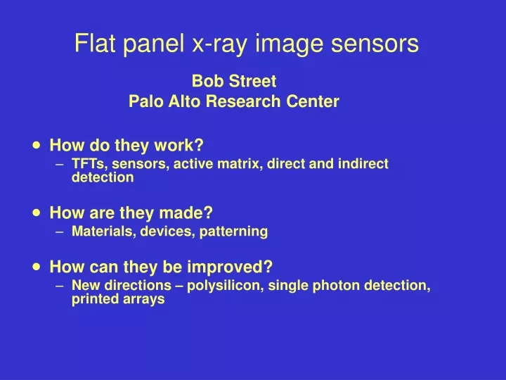
Flat panel x-ray image sensors. Bob Street Palo Alto Research Center How do they work? TFTs, sensors, active matrix, direct and indirect detection How are they made? Materials, devices, patterning How can they be improved?

E N D
Flat panel x-ray image sensors Bob Street Palo Alto Research Center How do they work? TFTs, sensors, active matrix, direct and indirect detection How are they made? Materials, devices, patterning How can they be improved? New directions – polysilicon, single photon detection, printed arrays
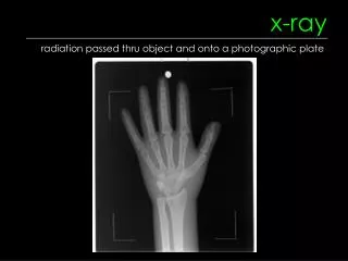
Radiography, fluoroscopy, mammography, radiation therapy, CT, quality control, security screening. Up to 40x40 cm active area, 10,000,000 pixels, 16 bit dynamic range, 2000 electron noise Flat panel x-ray imaging X-rays
Attributes of an image sensor Detection process • Sensitivity, dynamic range • X-ray conversion, electronic noise, etc • Spatial resolution • Pixel size, conversion process • Overall size • Pixel count, manufacturing process • Read out speed • Matrix addressing, capacitance, external electronics. X-rays Conversion; x-ray to charge Charge storage Charge readout substrate
Two modes of x-ray conversion Indirect detection Direct detection x-ray x-ray Voltage photo-excitation e e photo-excitation phosphor e.g. CsI photo- conductor ionization ionization recombination visible light a-Si array a-Si sensor array Good sensitivity (contact imaging). Reduced resolution due to light scattering. Simpler structure and materials. Potentially higher sensitivity. Better spatial resolution. More difficult materials.
Active matrix addressing gate shift register • The pixel capacitance stores the signal charge. • The TFT (off) holds the charge on the pixel. • The gate lines are addressed one at a time. • The TFT (on) passes the signal from the column of pixel to the data line • Readout resets the pixel capacitor • N2 pixels are read out with 2N contacts Data output bias TFT is on for 10-30 ms and off for 15-1000 ms
A-Si:H sensor array (indirect) Side view illumination Bias contact ITO Passivation p photodiode ~1 mm i TFT n a-Si:H silicon nitride data gate gate line photodiode TFT data line Bias line Top view
Materials and devices • A-Si and poly-Si Thin film transistors • Device processing • A-Si p-i-n photodiodes • Charge collection.
VSD, ISD VG Passiv. drain source channel insulator gate A-Si:H TFTs • Mobility 0.5-1cm2/Vsec • mA on-current. • Very high on/off ratio (1010) • Low threshold voltage • Moderate sub-threshold slope • On-off voltage swing is 10-15V • Small bias-stress effect above threshold sub-threshold TFT current ISD/VD = (W/L)CGmF (VG-VT) leakage Conduction = geometry . mobility . voltage
Glass Substrate Glass Substrate TFT Fabrication (an example) • Amorphous silicon thin film deposition is scalable to large area • Low temperature process for glass substrate • Channel, dielectric and passivation are deposited together. • a-Si:H ~50 nm • dielectric ~300nm 1. Pattern gate electrode Gate 2. Thin film deposition Nitride passivation a-Si:H SiN gate dielectric
Glass Substrate Glass Substrate UV Metal N+ a-Si:H TFT Fabrication 3. Self-aligned passivation etch • The etch exposes the channel for the contacts • Self-aligned for low capacitance. • N+ layer for leakage barrier. • Metal for low resistance 4. Patterning source/drain contacts
n+, p+ Polysilicon TFT Channel Si (50 nm) Oxide (700 nm) Glass Substrate Laser Laser recrystallization Dielectric, gate, dopant implant Gate passivation, contacts Source Channel Drain
Mobility ~100 cm2/Vsec CMOS capability Higher leakage current Dual gate Used for driver integration and pixel amplifiers Polysilicon TFT
a-Si p-i-n photodiodes ITO p+ a-Si:H 10 nm i a-Si:H 1-2 mm n+ a-Si:H 20 nm metal • Reverse bias • Large charge collection • Independent of bias • Peak sensitivity at 500-600 nm • Low leakage current • leakage mechanisms; bulk, contact, edge p-i-n photodiode
Charge collection V • Charge collection depends on mobility-lifetime () product • Material property related to trap density Values of V when V/d2= 1 eh X trap d 1 FQ 0 a-Si direct det. V
Photodiode leakage current • Sources of leakage current:- • Bulk defects • Contact injection • Edge leakage • Sensitive to processing • Reduced to 0.1 pA/mm2 Sensor reverse bias current - dependence on passivation
Indirect detection arrays • Pixel circuit • Device requirements • TFT • capacitance • Signal to noise • High fill factor design
1 fill factor 0 100 200 pixel size (micron) Indirect detection Bias voltage photodiode Bias lines • A-Si:H p-i-n photodiode provides pixel storage capacitance • Fill-factor = area of pixel covered by sensor. Storage capacitor Gate line data lines a-Si:H TFT TFT sensor Data line Gate lines Pixel circuit (simple)
C Ron TFT requirements Assumptions: Pixel capacitance 1 pF; 1000 gate lines; 30 fps 1. TFT ON Charge must transfer quickly to data line • Pixel RONC time-constant 2 sec • RON 2 Mohm • TFT with W/L 1.5 • Current requirement is easily met with mobility 1 cm2/Vsec
TFT requirements (cont) 2. TFT OFF Charge must remain on the pixel during integration • ROFFC > 100 sec (<1% discharge) • ROFF > 1014W • Very low TFT off-current is required • On/off ratio ~108
Capacitance effects • TFT parasitic capacitance • Puts feed-through charge on the pixel • Gate and data line capacitance • Reduces addressing speed • contributes to noise • Low capacitance improves performance • Self-aligned TFTs • Thick isolation layers Many sources of capacitance
C R Electronic noise Sources of noise • Data line capacitance to external preamplifiers • Noise = A+bCD • Depends on readout ASIC • Pixel kTC noise • Data line resistance • Power supply fluctuations • Array capacitance ext. amp. CD
Sensor Passivation Metal Gate Contact High fill factor sensor arrays • Continuous sensor layer • 3-d structure • Improves fill factor • Avoids sensor side walls • Lateral leakage can be controlled Top view Visible light image
Direct detection • Direct detection arrays • Material requirements • Se and HgI2 • Sensitivity and loss mechanisms • Charge collection
Direct detection array • Thick photoconductor replaces phosphor+photodiode • Active matrix array with added capacitor electrode TFT bias V gate line electrode Cross-section TFT capacitor data line
Direct detection material requirements • X-ray absorption • 200-500+ micron thick • High atomic number material • Charge collection • high mt products • Low leakage current • Low image lag • Large area deposition • Amorphous or polycrystalline • Evaporated, sputtered, screen-print… • Continuous film Top Metal Photoconductor Passivation Capacitor Bottom Metal Ground TFT Gate Line S/D Metal Data Line Material choices:- a-Se, PbI2, HgI2, CdZnTe
Selenium direct detection • Amorphous selenium deposited by vacuum evaporation • Doped with As and Cl to give good electron and hole charge collection • Ionization/collection is strongly field dependent • High operating voltages • Charge trapping at pixel boundaries • Illumination between frames
HgI2 films; a new alternative • Vacuum deposition or particle-in-binder • Polycrystalline layer; grain size 20->50 m • Blocking layer to protect against chemical reactions. • High x-ray absorption • Good LSF • Low leakage current • Several issues yet to resolve Line-spread function of HgI2
HgI2 x-ray response • High electron charge collection at low bias. • Higher sensitivity than other materials • Linear response Charge collection versus bias 250 mm film Good fit to charge collection formula
Charge collection corrections • Three loss components:- • Electron trapping (mt, V) • Absorption depth (kVp) • Small hole contribution (mt, V) 80 kVp 25 kVp Sum of positive and negative bias total electron collection. positive data represents loss Hole mt measured by correcting for electrons
Sensitivity evaluation WEFF before and after correction for x-ray absorption • Effective ionization energy, WEFF • Sensitivity ~ 1/WEFF • Max sensitivity when WEFF = W (=~5 eV) • Intrinsic sensitivity approaches theoretical maximum • Losses understood
Power Logic ADCs Gate shift register Digital data Readout amplifiers Active area Next generation image sensors? • Single photon detection • HgI2 • GEM amplifiers • Polysilicon arrays • Pixel amplifiers • Integrated drivers • New backplane technology • Printed arrays • Organic semiconductors
Single photon detection – HgI2 • First detection of single photons by a flat panel solid state detector. • Energy resolution needs to be improved • Low hole collection • Noise from dark current 512x512 array 100 mm pixel HgI2 detector photo-peak dark
GEM detectors with a-Si arrays • Single photon detection using GEM (gas electron multiplier) with a-Si:H backplane array • Gain of ~10,000 • Observation of x-ray polarization • Example of novel gain structure for single photon detection A-Si array to collect charge Images of 4-20 keV x-ray photons, measured with a-Si array GEM detector
To gate line Electronic integration with polysilicon • Integration of drive electronics • Shift register to drive TFT gates • Output multiplexer/amplifier to simplify readout. One stage of shift register 1mm First polysilicon image sensor array 384x256 array; 90 mm pixel
Vcc data line Sensor on top reset bias 3 TFT circuit gate line Polysilicon pixel amplifier • Demonstrated in 256x384 pixel array • 3 TFT follower circuit • 800 e noise • Needs 3-d sensor structure • Reduces sensitivity to external noise sources Poly-Si sensor arrays with pixel amplifier
Direct Write Etch Mask Deposit film Print wax mask Print head Heated sample holder Etch film strip wax Registration camera x-y stage a-Si TFT arrays fabricated by jet-printing • Digital lithography; maskless; software registration • Wax ink; feature size control • Multi-ejector print-head; high print speed Jet-printer
d 100 mm s G Jet-printed a-Si TFT array Gate layer Line width 30-40 mm Registration ~ 5 mm Island layer Source/drain layer TFT
300 mm Data Line s d Gate Line Printed a-Si TFT array • 64×64 matrix addressed array • Carrier mobility ~ 0.9 cm2 V-1s-1 • Extension to poly-silicon. • Could be used for large pixel applications
Polymer transistors Xerox poly(thiophene) W/L = 500/120 mm 'spun' on OTS-8 annealed at 150 C m =0.07 cm2V-1s-1 (linear & sat.) ON/OFF ~ 106 • Mobility is approaching a-Si • Simple deposition • Spin coat, print etc. • Unknown stability, lifetime, radiation hardness
Poly-Si TFT array Printed a-Si Summary - progress in large-area electronics Digital Lithography Poly-Silicon Medical imaging Printed Organic Arrays AMLCD Organic TFTs Amorphous Si 1980 1990 2000