Download
1 / 18
180 likes | 344 Views
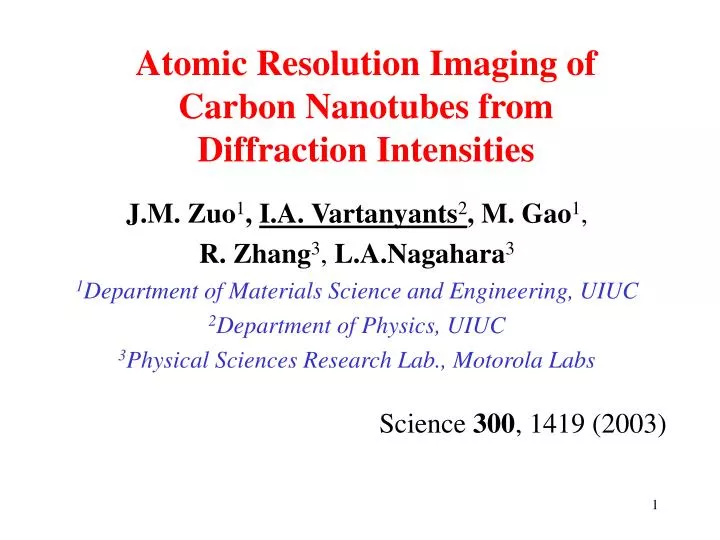
Atomic Resolution Imaging of Carbon Nanotubes from Diffraction Intensities. J.M. Zuo 1 , I.A. Vartanyants 2 , M. Gao 1 , R. Zhang 3 , L.A.Nagahara 3 1 Department of Materials Science and Engineering, UIUC 2 Department of Physics, UIUC 3 Physical Sciences Research Lab., Motorola Labs.

E N D
Atomic Resolution Imaging of Carbon Nanotubes from Diffraction Intensities J.M. Zuo1, I.A. Vartanyants2, M. Gao1, R. Zhang3, L.A.Nagahara3 1Department of Materials Science and Engineering, UIUC 2Department of Physics, UIUC 3Physical Sciences Research Lab., Motorola Labs Science 300, 1419 (2003)
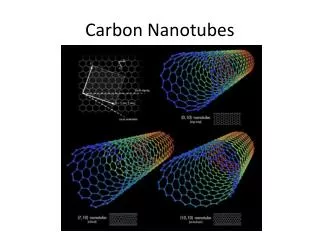
Carbon Nanotubes (atomic structure) c=na1+ma2, c – wrapping vector, a1, a2– unit vectors • n=m – ‘armchair’ • m=0 – ‘zigzag’ STM images of single-walled nanotubes J. Wildoer, et al, Science, 391, 59 (1998).
Carbon Nanotubes (imaging) • Structure: A – armchair B - zigzag C – chiral • Imaging: D – STM image of 1.3 nm SWNT (J. Wildoer et al., Science 391, 59 (1998)) E – TEM image of MWNT F – TEM micrograph of 1.4 nm SWNTs in a bundle (A. Thess et al., Science 273, 483 (1996) G – SEM image of MWNTs grown as a nanotube forest
Coherent Nano-Area Electron Diffraction Schematic ray diagram CL – condenser lens CA – condenser aperture FP – front focal plane OL – objective lens D – imaging plates
Electron Scattering on Carbon Nanotubes Weak phase object – kinematic scattering Transmission function Diffracted intensity: For constant illumination: (r)=const
Electron wavefront on the sample 10 m aperture Cs and f – spherical aberration and defocus of electron lens
Electron Diffraction pattern from SWNT Scattering amplitude for SWNT: Experiment diffraction pattern d=1.40±0.02 nm, =17.0º(±0.2º) Simulated diffraction pattern (n1, n2)=(14, 6) d=1.39 nm, =17.0º M. Gao, J.M. Zuo et al., Appl. Phys. Lett (2003)
Iterative phase retrieval algorithm FFT sk(x) Ak(q) Real Space Constraints Reciprocal Space Constraints s'k(x) A'k(q) FFT-1 • Real space constraints: • finite support • real, positive Reciprocal space constraint: R.W.Gerchberg & W.O. Saxton, Optic (1972) 35, 237 J.R. Fienup, Appl Opt. (1982). 21, 2758 R.P. Millane & W.J. Stroud, J. Opt. Soc. Am. (1997) A14, 568
Reconstruction of SWNT from simulated data Simulated diffraction pattern Reconstructed Image
Reconstruction of SWNT Experimental Diffraction Pattern Reconstructed Diffraction Pattern
Far-field diffraction pattern from DWNT Pixel resolution 0.025 1/nm
1d reconstruction from DWNT Equatorial data Reconstructed electron density
Electron Diffraction Pattern from DWNT Experiment Reconstruction
Reconstructed Image and model of DWNT Model Outer tube: (n1,n2)=(35,25) d1=4.09 nm Inner tube: (n1,n2)=(26,24) d2=3.39 nm
Possible Applications • Imaging of biological molecules • ferritine, • actines, • radiation damage • Imaging of nanostructures • nanowires • nanoclusters