Download
1 / 73
730 likes | 737 Views
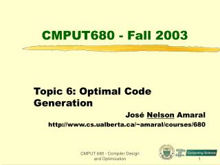
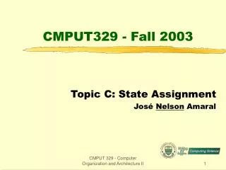
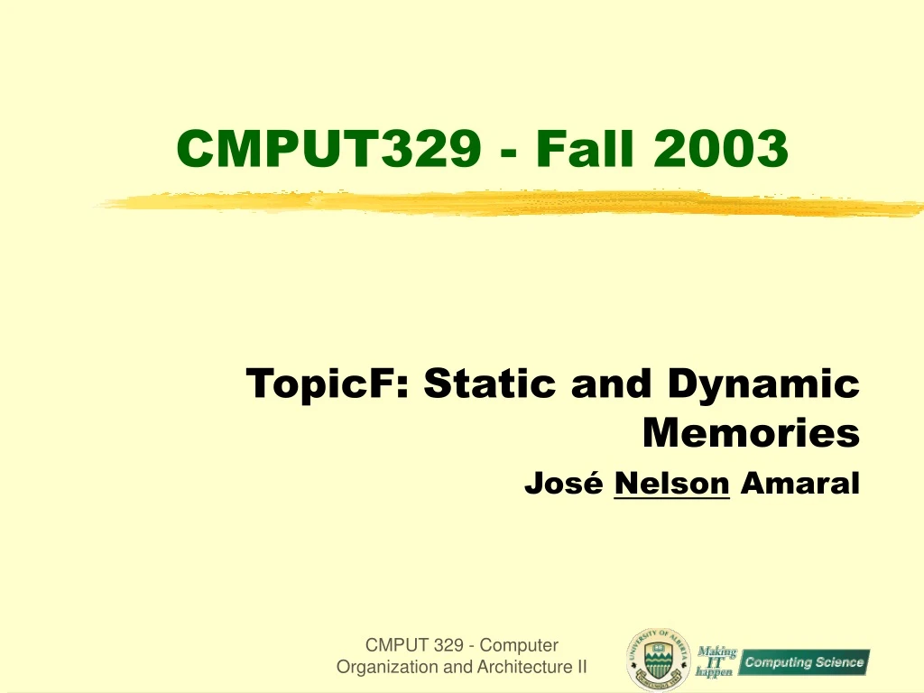
CMPUT329 - Fall 2003. TopicF: Static and Dynamic Memories José Nelson Amaral. Reading Assignment. Chapter 10 of Wakerly. Sections 10.1, 10.2, 10.3, 10.4. 0 1 2. M u x. 0. 0. M u x. M u x. 1. 1. 0. M u x. 0 1 2 3. 1. M u x. 32. 32. 16. 26. 4. ALUOp. PcWrite.

E N D
CMPUT329 - Fall 2003 TopicF: Static and Dynamic Memories José Nelson Amaral CMPUT 329 - Computer Organization and Architecture II
Reading Assignment Chapter 10 of Wakerly Sections 10.1, 10.2, 10.3, 10.4 CMPUT 329 - Computer Organization and Architecture II
0 1 2 M u x 0 0 M u x M u x 1 1 0 M u x 0 1 2 3 1 M u x 32 32 16 26 4 ALUOp PcWrite Control Unit PcWriteCond PCSource IorD ALUSelA MemRead TargetWrite RegWrite MemWrite Target IRWrite MemtoReg ALUSelB RegDst Conc/ Shift left 2 PC I[25-21] Read register 1 Read address Instruction [31-26] Read data 1 I[20-16] Zero Read register 2 Memory Write address ALU result Instruction [25-0] Write register Read data 2 ALU MemData Instruction register 4 Write data Write data [15-11] Registers 0 M u x 1 32 ALU control Sign ext. I[15-0] Shift left 2
0 1 2 M u x 0 0 M u x M u x 1 1 0 M u x 0 1 2 3 1 M u x 32 32 16 26 4 ALUOp PcWrite Control Unit PcWriteCond PCSource IorD ALUSelA MemRead TargetWrite RegWrite MemWrite Target IRWrite MemtoReg ALUSelB RegDst Conc/ Shift left 2 PC I[25-21] Read register 1 Read address Instruction [31-26] Read data 1 I[20-16] Zero Read register 2 Memory Write address ALU result Instruction [25-0] Write register Read data 2 ALU MemData Instruction register 4 Write data Write data [15-11] Registers 0 M u x 1 32 ALU control Sign ext. I[15-0] Shift left 2
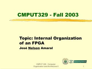
8K 8 16K 8 32K 8 64K 8 2764 27128 27256 27512 A0 A0 A0 A0 A0 A0 A0 A0 A1 A1 A1 A1 A1 A1 A1 A1 • • • • • • • • • • • • D0 D0 D0 D0 A14 A14 A14 A14 O0 O0 O0 O0 A12 A13 A14 A15 D1 D1 D1 D1 O1 O1 O1 O1 • • • • • • • • • • • • O7 O7 O7 O7 CS CS CS CS D7 D7 D7 D7 OE OE OE OE EPROMs(Erasable Programmable Read Only Memories) A0-A15: Address Bus D0-D7: Data Bus CS: Chip Select OE: Output Enable CMPUT 329 - Computer Organization and Architecture II
27256 A0 A0 A1 A1 • • • D0 A14 O0 A14 D1 O1 • • • O7 CS D7 OE Address Decoding on a Microprocessor System microprocessor A0 A1 • • • A19 74x139 1Y0 1Y1 1Y2 1Y3 1G 1A 1B D0 D1 • • • D7 READ WRITE CMPUT 329 - Computer Organization and Architecture II
1Y0_L 1G_L 74x139 1Y1_L 4 1 1Y0 1Y1 1Y2 1Y3 1G 2G 5 2 6 1A 1B 2A 2B 13 7 1Y2_L 12 15 2Y0 2Y1 2Y2 2Y3 11 14 10 1A 1Y3_L 13 9 1B The 74x139 Decoder CMPUT 329 - Computer Organization and Architecture II
1Y0_L 1G_L 1Y1_L 1Y2_L 1A 1Y3_L 1B The 74x139 Decoder CMPUT 329 - Computer Organization and Architecture II
1Y0_L 1G_L 1Y1_L 1Y2_L 1A 1 1Y3_L 1B 0 The 74x139 Decoder CMPUT 329 - Computer Organization and Architecture II
1Y0_L 1G_L 1Y1_L 1Y2_L 1A 1 1Y3_L 1B 0 The 74x139 Decoder CMPUT 329 - Computer Organization and Architecture II
1 0 The 74x139 Decoder 1Y0_L 1G_L 1Y1_L 1Y2_L 1A 1Y3_L 1B CMPUT 329 - Computer Organization and Architecture II
1 0 The 74x139 Decoder 1Y0_L 1G_L 1Y1_L 1Y2_L 1A 1Y3_L 1B CMPUT 329 - Computer Organization and Architecture II
1 0 The 74x139 Decoder 1Y0_L 1G_L 1Y1_L 1Y2_L 1A 1Y3_L 1B CMPUT 329 - Computer Organization and Architecture II
1Y0_L 1G_L 1Y1_L 1Y2_L 1A 1Y3_L 1B The 74x139 Decoder CMPUT 329 - Computer Organization and Architecture II
74x139 4 1 1Y0 1Y1 1Y2 1Y3 1G 2G 5 2 6 1A 1B 2A 2B 13 7 12 15 2Y0 2Y1 2Y2 2Y3 11 14 10 13 9 The 74x139 Decoder CMPUT 329 - Computer Organization and Architecture II
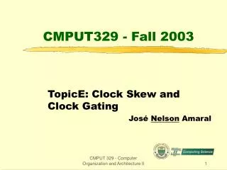
Address Decoding We want to design a microprocessor-based system with 128 Kbytes of EPROM using the 27256 EPROM chips that have an organization of 32K 8 bits. This particular microprocessor has a data bus that is 8-bit wide and an address bus that is 20-bits wide. The EPROM is to be mapped to the highest addresses of the memory address space. CMPUT 329 - Computer Organization and Architecture II
14 15 13 19 18 16 17 11 14 12 11 10 10 12 13 6 7 9 8 1 2 1 5 3 3 2 0 4 5 4 6 7 9 8 0 Therefore, the 32K highest addresses in this memory system have the following addresses. 19 18 17 16 15 1 1 1 1 1 Address Decoding A memory address in this system has the following format: 32 Kbytes = 32 1024 = 25 210 = 215 bytes Thus we need 15 address lines to address 32 Kbytes. CMPUT 329 - Computer Organization and Architecture II
13 11 10 12 13 14 10 12 14 11 2 6 7 8 9 4 1 3 2 5 5 4 6 7 9 3 8 0 1 0 19 19 18 18 17 17 16 16 15 15 1 1 1 1 1 1 1 Address Decoding The 64K highest addresses are the following addresses. And the 128K highest addresses are: CMPUT 329 - Computer Organization and Architecture II
11 14 12 13 10 9 7 6 4 8 3 2 0 1 5 A19 HIMEN_L A18 19 18 17 16 15 A17 1 1 1 Address Decoding Thus to verify if a memory access is to the EPROM region, we can just verify if the address lines A19, A18, and A17 are simultaneously 1: CMPUT 329 - Computer Organization and Architecture II
Address Decoding To create a space of 128 Kbytes of EPROM with chips that have 32 Kbytes capacity, we will need four memory chips. How can we use the address lines to identify which memory chip is been accessed each time? CMPUT 329 - Computer Organization and Architecture II
19 18 17 16 15 14 13 12 11 10 9 8 7 6 5 4 3 2 1 0 19 18 17 16 15 14 13 12 11 10 9 8 7 6 5 4 3 2 1 0 1 1 1 1 1 1 1 1 1 1 1 1 1 1 1 1 1 1 1 1 1 1 1 1 1 0 0 0 0 0 0 0 0 0 0 0 0 0 0 0 And ending at: FFFFF Address Decoding The memory chip placed at the higher portion of the address space contains the memory addresses starting at: F8000 CMPUT 329 - Computer Organization and Architecture II
Bank 1 Bank 2 E8000 F0000 EFFFF F7FFF 1 1 1 1 1 1 0 1 0 1 1 1 1 1 1 1 1 1 1 1 1 1 1 1 1 1 1 1 1 1 1 1 1 1 1 1 1 1 1 1 19 19 19 19 18 18 18 18 17 17 17 17 16 16 16 16 15 15 15 15 14 14 14 14 13 13 13 13 12 12 12 12 11 11 11 11 10 10 10 10 9 9 9 9 8 8 8 8 7 7 7 7 6 6 6 6 5 5 5 5 4 4 4 4 3 3 3 3 2 2 2 2 1 1 1 1 0 0 0 0 1 1 1 1 1 1 1 1 1 1 1 1 1 0 1 0 1 1 0 0 0 0 0 0 0 0 0 0 0 0 0 0 0 0 0 0 0 0 0 0 0 0 0 0 0 0 0 0 0 0 0 0 0 0 0 0 0 0 0 0 0 0 0 0 0 0 0 0 0 0 0 0 0 0 0 0 0 0 0 0 Address Decoding Bank 3 F8000 FFFFF 1 1 1 1 1 1 1 1 1 1 1 1 1 1 1 1 1 1 1 1 Bank 0 E0000 E7FFF 1 1 1 0 0 1 1 1 1 1 1 1 1 1 1 1 1 1 1 1 CMPUT 329 - Computer Organization and Architecture II
Address Decoding 19 18 17 16 15 14 13 12 11 10 9 8 7 6 5 4 3 2 1 0 Bank 3 F8000 1 1 1 1 1 0 0 0 0 0 0 0 0 0 0 0 0 0 0 0 FFFFF 1 1 1 1 1 1 1 1 1 1 1 1 1 1 1 1 1 1 1 1 19 18 17 16 15 14 13 12 11 10 9 8 7 6 5 4 3 2 1 0 Bank 2 F0000 1 1 1 1 0 0 0 0 0 0 0 0 0 0 0 0 0 0 0 0 F7FFF 1 1 1 1 0 1 1 1 1 1 1 1 1 1 1 1 1 1 1 1 19 18 17 16 15 14 13 12 11 10 9 8 7 6 5 4 3 2 1 0 Bank 1 E8000 1 1 1 0 1 0 0 0 0 0 0 0 0 0 0 0 0 0 0 0 EFFFF 1 1 1 0 1 1 1 1 1 1 1 1 1 1 1 1 1 1 1 1 19 18 17 16 15 14 13 12 11 10 9 8 7 6 5 4 3 2 1 0 Bank 0 E0000 1 1 1 0 0 0 0 0 0 0 0 0 0 0 0 0 0 0 0 0 E7FFF 1 1 1 0 0 1 1 1 1 1 1 1 1 1 1 1 1 1 1 1 CMPUT 329 - Computer Organization and Architecture II
A19 SE0000_L HIMEN_L A18 SE8000_L A17 SF0000_L A15 A16 SF8000_L Address Decoding on a Microprocessor System microprocessor 27256 27256 27256 27256 A0 A0 A0 A0 A0 A0 A0 A0 A0 A0 A1 A1 A1 A1 A1 A1 A1 A1 A1 A1 • • • • • • • • • • • • D0 D0 D0 D0 A14 A14 A14 A14 O0 O0 O0 O0 • • • A14 A14 A14 A14 D1 D1 D1 D1 O1 O1 O1 O1 • • • • • • • • • • • • A19 A19 O7 O7 O7 O7 CS CS CS CS D7 D7 D7 D7 OE OE OE OE D0 D0 D1 D1 • • • D7 D7 READ 74x139 1Y0 1Y1 1Y2 1Y3 WRITE 1G 1A 1B
Types of Memories Read/Write Memory (RWM): we can store and retrieve data. the time required to read or write a bit of memory is independent of the bit’s location. Random Access Memory (RAM): once a word is written to a location, it remains stored as long as power is applied to the chip, unless the location is written again. Static Random Access Memory (SRAM): the data stored at each location must be refreshed periodically by reading it and then writing it back again, or else it disappears. Dynamic Random Access Memory (DRAM): CMPUT 329 - Computer Organization and Architecture II
In principle, in a RAM, all positions of the memory can be read on a random fashion with approximately the same delay for all positions. However, modern RAMs allow burst accesses that favor sequential accesses (complete them in less time). Random Access Memories (RAMs) A Random-Access Memory (RAM) is so called to contrast with its predecessor, the Serial-Access Memory. In a serial access memory, memory positions become available for reading on a sequential fashion. Therefore to read an specific memory position, the reader must wait a variable time delay for the memory position to became available. CMPUT 329 - Computer Organization and Architecture II
The following control inputs are typically used to control a Static-RAM. Output Enable (OE): Enable the output into the data lines Chip Select (CS): Used in connection with OE to simplify the design of a multiple chip system. Write Enable (WE): When asserted, the data inputs are written to the selected memory location. Static-RAM Control Inputs The outputs of memory chips are often connected to a three-state bus, a bus that can be driven by many devices. Therefore each memory chip should drive the bus only when commanded to do so by the control logic. CMPUT 329 - Computer Organization and Architecture II
DIN0 A0 DIN1 A1 Address inputs Data inputs DOUT0 DOUT1 DINb-1 An-1 DOUTb-1 A 2nb SRAM 2n b SRAM Data outputs CS control inputs OE WE CMPUT 329 - Computer Organization and Architecture II
HM6264 2764 A0 A0 A1 A1 • • • D0 IO0 A12 A12 D1 IO1 • • • CS CS1 WE CS WE WE CS2 CS1 CS2 WE D7 IO7 OE OE OE OE SRAMs(Static Random Access Memories) HM62256 HM628128 HM628512 2764 2764 2764 A0 A0 A0 A0 A0 A0 A1 A1 A1 A1 A1 A1 • • • • • • • • • D0 D0 D0 IO0 IO0 IO0 A14 A16 A18 A14 A16 A18 D1 D1 D1 IO1 IO1 IO1 • • • • • • • • • D7 D7 D7 IO7 IO7 IO7 CMPUT 329 - Computer Organization and Architecture II
Accesses to SRAM Read An address is placed on the address inputs while CS and OE are asserted. The latch outputs for the selected memory locations are delivered to DOUT. Write An address is placed on the address inputs and a data word is placed on DIN; then CS and WE are asserted. The latches in the selected memory location open, and the input word is stored. CMPUT 329 - Computer Organization and Architecture II
0 1 2 3 4 5 6 7 DIN2 DIN0 DIN3 DIN1 IN OUT SEL WR IN OUT SEL WR IN OUT SEL WR IN OUT SEL WR 3-to-8 decoder IN OUT SEL WR IN OUT SEL WR IN OUT SEL WR IN OUT SEL WR IN OUT SEL WR IN OUT SEL WR IN OUT SEL WR IN OUT SEL WR 0 1 1 A2 A1 A0 2 1 0 IN OUT SEL WR IN OUT SEL WR IN OUT SEL WR IN OUT SEL WR IN OUT SEL WR IN OUT SEL WR IN OUT SEL WR IN OUT SEL WR IN OUT SEL WR IN OUT SEL WR IN OUT SEL WR IN OUT SEL WR IN OUT SEL WR IN OUT SEL WR IN OUT SEL WR IN OUT SEL WR IN OUT SEL WR IN OUT SEL WR IN OUT SEL WR IN OUT SEL WR WR_L WE_L CS_L IOE_L OE_L DOUT3 DOUT2 DOUT1 DOUT0
0 1 2 3 4 5 6 7 DIN3 DIN3 DIN3 DIN3 IN OUT SEL WR IN OUT SEL WR IN OUT SEL WR IN OUT SEL WR 3-to-8 decoder IN OUT SEL WR IN OUT SEL WR IN OUT SEL WR IN OUT SEL WR IN OUT SEL WR IN OUT SEL WR IN OUT SEL WR IN OUT SEL WR 0 1 1 A2 A1 A0 2 1 0 IN OUT SEL WR IN OUT SEL WR IN OUT SEL WR IN OUT SEL WR IN OUT SEL WR IN OUT SEL WR IN OUT SEL WR IN OUT SEL WR IN OUT SEL WR IN OUT SEL WR IN OUT SEL WR IN OUT SEL WR IN OUT SEL WR IN OUT SEL WR IN OUT SEL WR IN OUT SEL WR IN OUT SEL WR IN OUT SEL WR IN OUT SEL WR IN OUT SEL WR WR_L WE_L CS_L IOE_L OE_L DOUT3 DOUT3 DOUT3 DOUT3
0 1 2 3 4 5 6 7 DIN3 DIN3 DIN3 DIN3 IN OUT SEL WR IN OUT SEL WR IN OUT SEL WR IN OUT SEL WR 3-to-8 decoder IN OUT SEL WR IN OUT SEL WR IN OUT SEL WR IN OUT SEL WR IN OUT SEL WR IN OUT SEL WR IN OUT SEL WR IN OUT SEL WR 0 1 1 A2 A1 A0 2 1 0 IN OUT SEL WR IN OUT SEL WR IN OUT SEL WR IN OUT SEL WR IN OUT SEL WR IN OUT SEL WR IN OUT SEL WR IN OUT SEL WR IN OUT SEL WR IN OUT SEL WR IN OUT SEL WR IN OUT SEL WR IN OUT SEL WR IN OUT SEL WR IN OUT SEL WR IN OUT SEL WR IN OUT SEL WR IN OUT SEL WR IN OUT SEL WR IN OUT SEL WR WR_L WE_L CS_L IOE_L OE_L DOUT3 DOUT3 DOUT3 DOUT3
0 1 2 3 4 5 6 7 DIN3 DIN3 DIN3 DIN3 IN OUT SEL WR IN OUT SEL WR IN OUT SEL WR IN OUT SEL WR 3-to-8 decoder IN OUT SEL WR IN OUT SEL WR IN OUT SEL WR IN OUT SEL WR IN OUT SEL WR IN OUT SEL WR IN OUT SEL WR IN OUT SEL WR 0 1 1 A2 A1 A0 2 1 0 IN OUT SEL WR IN OUT SEL WR IN OUT SEL WR IN OUT SEL WR IN OUT SEL WR IN OUT SEL WR IN OUT SEL WR IN OUT SEL WR IN OUT SEL WR IN OUT SEL WR IN OUT SEL WR IN OUT SEL WR IN OUT SEL WR IN OUT SEL WR IN OUT SEL WR IN OUT SEL WR IN OUT SEL WR IN OUT SEL WR IN OUT SEL WR IN OUT SEL WR WR_L WE_L CS_L IOE_L OE_L DOUT3 DOUT3 DOUT3 DOUT3
SRAM with Bi-directional Data Bus microprocessor IN OUT SEL WR IN OUT SEL WR IN OUT SEL WR IN OUT SEL WR WR_L WE_L CS_L IOE_L OE_L DIO3 DIO2 DIO1 DIO0 CMPUT 329 - Computer Organization and Architecture II
Internal Address Decoding The SRAM shown in the previous slides had 3 address lines and stored 8 words, requiring a 3-to-8 internal decoder. Such a decoder requires eight AND gates, with three inputs each, and three inversors. Consider the HM628512 SRAM that has 19 address lines and stores 512K words. What size internal decoder this chip requires? A 19-to-512K decoder with 524288 AND gates, each with 19 inputs? CMPUT 329 - Computer Organization and Architecture II
Internal Address Decoding To avoid such a complexity in the decoding logic, all memories (EPROMs, SRAMs, and DRAMs) use two-dimensional decoding which reduces the decoder size to approximately the square root of the number of addresses. The memory cells are organized in a two-dimensional array. Some address lines are used to select a row and the others are used to select a column. The cell selected by the whole address is at the intersection of the row and the column. CMPUT 329 - Computer Organization and Architecture II
Static-RAM Read Timing tAA (access time for address): how long it takes to get stable output after a change in address. tACS (access time for chip select): how long it takes to get stable output after CS is asserted. tOE (output enable time): how long it takes for the three-state output buffers to leave the high-impedance state when OE and CS are both asserted. tOZ (output-disable time): how long it takes for the three-state output buffers to enter high-impedance state after OE or CS are negated. tOH (output-hold time): how long the output data remains valid after a change to the address inputs. CMPUT 329 - Computer Organization and Architecture II
tAA Max(tAA, tACS) tOE tOZ tACS tAA tOH tOZ Static-RAM Read Timing ADDR stable stable stable CS_L OE_L tOE DOUT valid valid valid WE_L = HIGH CMPUT 329 - Computer Organization and Architecture II
Static-RAM Write Timing tAS (address setup time before write): all address inputs must be stable at this time before both CS and WE are asserted. tAH(address hold time after write): all address inputs must be held stable until this time after CS or WE is negated. tCSW (chip-select setup before end of write): CS must be asserted at least this long before the end of the write cycle. tWP (write pulse width): WE must be asserted at least this long to reliably latch data into the selected cell. tDS (data setup time before end of write): All of the data inputs must be stable at this time before the write cycle ends. tDH (data hold time after the end of write): All data inputs must be held stable until this time after the write cycle ends. CMPUT 329 - Computer Organization and Architecture II
To deliver the higher memory density required for computer systems, a single transistor memory cell was developed. bit line word line 1-bit DRAM cell Dynamic Memory Cell An SRAM cell has a bi-stable latch that requires from four to six transistors to be built. CMPUT 329 - Computer Organization and Architecture II
bit line word line 1-bit DRAM cell Writing 1 in a Dynamic Memories To store a 1 in this cell, a HIGH voltage is placed on the bit line, causing the capacitor to charge through the on transistor. CMPUT 329 - Computer Organization and Architecture II
bit line word line 1-bit DRAM cell Writing 0 in a Dynamic Memories To store a 0 in this cell, a LOW voltage is placed on the bit line, causing the capacitor to discharge through the on transistor. CMPUT 329 - Computer Organization and Architecture II
bit line word line 1-bit DRAM cell Destructive Reads To read the DRAM cell, the bit line is precharged to a voltage halfway between HIGH and LOW, and then the word line is set HIGH. Depending on the charge in the capacitor, the precharged bit line is pulled slightly higher or lower. A sense amplifier detects this small change and recovers a 1 or a 0. CMPUT 329 - Computer Organization and Architecture II
bit line word line 1-bit DRAM cell Recovering from Destructive Reads The read operation discharges the capacitor. Therefore a read operation in a dynamic memory must be immediately followed by a write operation of the same value read to restore the capacitor charges. CMPUT 329 - Computer Organization and Architecture II
bit line word line 1-bit DRAM cell Forgetful Memories The problem with this cell is that it is not bi-stable: only the state 0 can be kept indefinitely, when the cell is in state 1, the charge stored in the capacitor slowly dissipates and the data is lost. CMPUT 329 - Computer Organization and Architecture II
1 written refreshes Vcap VCC HIGH LOW 0V time 0 stored Refreshing the Memory The solution is to periodically refresh the memory cells by reading and writing back each one of them. CMPUT 329 - Computer Organization and Architecture II
If we would refresh each cell every 4 miliseconds we would have to perform a refresh operation every: Refreshing Frequency Each dynamic RAM cell must be refreshed at about every 4 miliseconds. Some commercial DRAMs contain 256 megabits. There would be no time for regular memory accesses!! How do we solve this problem? CMPUT 329 - Computer Organization and Architecture II
Refreshing Memory The DRAMs are organized in two dimensional arrays, and a single refreshing operation can refresh an entire row at a time. Newer DRAMs have 4096 rows, but only need to be refreshed every 64 miliseconds. Therefore they require one refresh operation about every 15.6 second. A refresh operation typically takes 100 nanoseconds. Therefore the memory is available for regular accesses more than 99% of the time. CMPUT 329 - Computer Organization and Architecture II
Internal Structure of a 64K 1 DRAM Row decoder 256 256 array row address column address A0-A7 control Column latches, multiplexers, and demultiplexers RAS_L CAS_L WE_L latch, mux, and dmux control DIN DOUT CMPUT 329 - Computer Organization and Architecture II