Download
1 / 22
430 likes | 999 Views
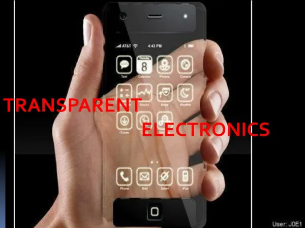
Transparent Electronics. Submitted by, Sajas K.K. Roll no: 18 S5 EC. Guided by Miss . Shahida. Introduction What is transparent electronics?

E N D
TransparentElectronics Submitted by, Sajas K.K. Roll no: 18 S5 EC Guided by Miss. Shahida
Introduction What is transparent electronics? • In transparent electronics the usual opaque semiconductor materials forming the basis for electronic device fabrication is replaced with transparent materials.
There are two technologies which preceded and underlie transparent electronics: • Transparent Conducting Oxides (TCOs) • Thin Film Transistors (TFTs)
Transparent Conducting Oxides TCOs) • TCOs constitute an unusual class of materials possessing two physical properties (generally considered mutually exclusive): • High optical transparency. ( Eg>3.1eV) • High electrical conductivity.
Transparent Passive devices • Transparent Thin Film Resistors • Transparent Thin Film Capacitors • Transparent Thin Film Inductors
Resistive material: ITO (Indium Tin Oxide) • Typical sheet resistance ~ 10- • Conductivity of TCO’s depends on number of oxygen vacancies ( and metal atoms occupying interstitial sites.
Most insulators are transparent. • Contact layer is made of highly conducting TCOs (ITO).
Transparent Thin Film Inductors • Hard to realize due to poor conductivity of TCO’s compared to metals. • High L requires larger number of turns which in turn results in increased parasitic resistance.
Schottky Barriers • Formed from metal (anode)-semiconductor (cathode) junction. • Space charge region (depletion region) and potential barrier formation due to difference in work function of metal and semiconductor. • Schottky barrier height , where Schottky barrier height work function of metal Electron affinity of semiconductor
Transparent Thin Film Transistors • Constitutes the heart of transparent electronics • Channel is formed from highly insulating, wide band gap transparent semiconductor(ZnO). • Source, drain and gate contacts are made from highly conductive TCO (ITO). • Two possible configurations are: • Bottom gate • Top gate
Possible structure, (a) Bottom gate, and (b) Top gate.
Applications • Active Matrix LCD (AMLCD). • Active Matrix Organic Light Emitting Device display backplane (AMOLED). • Value added glass. • Transparent electronics on opaque substrates.
UV detectors and arrays • Transparent solar cells • UV detectors for spectrally resolved imaging. • Security applications: Invisible cameras and Invisible RFID’s
Conclusion • Started as a mere electrical device technology during world war 2, transparent electronics now holds the key for many future advancements in security, entertainment efficient utilization of energy.
Reference • ‘Transparent Electronics ’, Springer publications, J.F.Wager, D. A. Keszler, R. E. Presley. • ‘Transparent electronics: from synthesis to applications’, Wiley publications: Antonio Facchetti, Tobin J. Marks