Download
1 / 16
790 likes | 1.85k Views
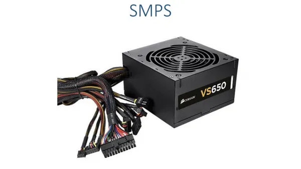
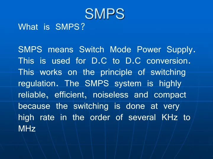
What is SMPS? SMPS means Switch Mode Power Supply. This is used for D.C to D.C conversion. This works on the principle of switching regulation. The SMPS system is highly reliable, efficient, noiseless and compact because the switching is done at very high rate in the order of several KHz to MHz.

E N D
What is SMPS? SMPS means Switch Mode Power Supply. This is used for D.C to D.C conversion. This works on the principle of switching regulation. The SMPS system is highly reliable, efficient, noiseless and compact because the switching is done at very high rate in the order of several KHz to MHz SMPS
Necessity The SMPS regulators are used in B.S.N.L at various locations like CDOT, E10B and Transmission systems etc.
SMPS Principle of Switching Regulator
A pulse train drives the base of ‘switching or pass transistor’. When the voltage to the base is high, the transistor saturates, when the voltage is low, the transistor turns off. Here the transistor functions as a switch. When the transistor is ON, load current is drawn through the transistor and choke L. When the transistor is OFF the load current is maintained by the energy stored in the choke L. The current flows through earth, Diode D, choke, load and earth. Hence this diode is called ‘Retrieval Diode’.
A pulse train drives the base of ‘switching or pass transistor’. When the voltage to the base is high, the transistor saturates, when the voltage is low, the transistor turns off. Here the transistor functions as a switch. When the transistor is ON, load current is drawn through the transistor and choke L. When the transistor is OFF the load current is maintained by the energy stored in the choke L. The current flows through earth, diode D, choke, load and earth. Hence this diode is called ‘retrieval diode’.
Duty cycle of the Transistor D = On Time On Time + Off Time (one cycle time) The output voltage = Input voltage x D
For example If I/P voltage is 200 volts and D=0.25 O/P voltage = 200 x 0.25 = 50V. Regulation is achieved by modifying the Duty cycle. Duty cycle depends on onetime of transistor, which in turn depends on the width of the pulse applied to the base of the transistor, which is controlled by ‘Pulse width modulation’ by regulator circuit
Regulation • The relaxation oscillator produces a square wave. The square wave is integrated to get a triangular wave, which drives the non-inverting input of a triangular to pulse converter. The pulse train out of this circuit then drives the Pass Transistor. The output is sampled by a voltage divider and fed to a comparator. The feed back voltage is compared with a reference voltage. The output of the comparator then drives the input of the triangular to pulse converter
Regulation If the output voltage tries to increase the comparator produces a higher output voltage which raises the reference voltage of the triangular- to pulse converter. This makes the pulse that drives the base of the switching transistor narrower. That means duty cycle is reduced. Since the duty cycle is lower the output becomes less which tries to cancel almost all the original increase in output voltage.
Regulation • Conversely, if the regulated output voltage tries to decrease, the output of the comparator decreases the reference voltage of the triangular -to pulse converter. This makes the pulse wider and the transistor conducts for larger time and more voltage comes out of the L.C.filter. This cancels out the original decrease in output voltage
Input Section Block 1 EMI Block 2 Current limiter Block 3 Floate Block 4 Power factor corrector 100khz Blokck 6-9 DC-DC converter
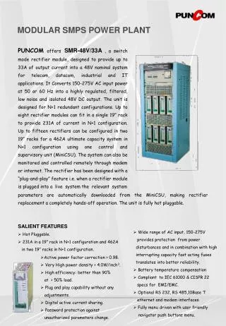
TELECOMMUNICATION ENGINEERING CENTRE (DOT) for the S.M.P.S. BASED POWER PLANT GENERIC REQUIREMENTS (No. G7SMP/-01/01 JULY 04) • Primary application of the rectifiers SMPS 48V-5600W are in the supply of Telecom equipment. The convection cooled unit may be operated up to 60oC ambient air temperature. • The rectifier operates from a nominal 3 X 230 Vacrms (with neutral wire) source. The mains frequency may vary from 45 Hz to 65 Hz. Total harmonic distortion (THD) of the input current wave form is below 5%.