Download
1 / 9
90 likes | 220 Views
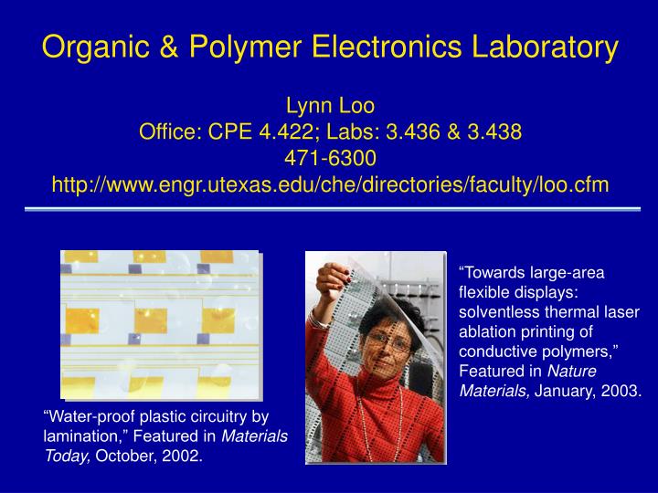
Organic & Polymer Electronics Laboratory Lynn Loo Office: CPE 4.422; Labs: 3.436 & 3.438 471-6300 http://www.engr.utexas.edu/che/directories/faculty/loo.cfm. “Towards large-area flexible displays: solventless thermal laser ablation printing of conductive polymers,”

E N D
Organic & Polymer Electronics Laboratory Lynn Loo Office: CPE 4.422; Labs: 3.436 & 3.438 471-6300 http://www.engr.utexas.edu/che/directories/faculty/loo.cfm “Towards large-area flexible displays: solventless thermal laser ablation printing of conductive polymers,” Featured in Nature Materials, January, 2003. “Water-proof plastic circuitry by lamination,” Featured in Materials Today, October, 2002.
Introduction: The World’s First Electronic Paper Rogers et al., Proc. Nat. Acad. Sci. USA 2001.
Backplane: Organic Transistors on Plastic Substrate Rogers et al., Proc. Nat. Acad. Sci. USA 2001.
Why Organic Materials and Plastic Substrates? • Improved mechanical flexibility and bendability • Large-area coverage • Compatible with high-speed reel-to-reel fabrication • Low production costs • Potential applications in large-area flexible displays, disposable RF • tags, wearable electronics, etc. • e.g., the first OLED active matrix display digital camera by Kodak • (March, 2003) Kodak LS 633 http://www.kodak.com
Group Focus • Design and synthesis of new materials for electronic applications (Bucholz, Guloy, Smith) • Understanding structure-property interrelationships and how they can impact device performance (Krapchetov, Lee, Khan) • Developing unconventional, non-invasive materials processing, patterning, and printing technologies specifically for organic device fabrication (Felmet, Lee, Mitchell)
Organic and Polymer Electronics Laboratory Design & Synthesis of Functional Polymers Structure & Property Relationships Device Fabrication & Testing 1 polymer chemistry/physics project available; can be co-advised with Prof. Ganesan 1 patterning project available SMM TLB KSL MFK QAS ASG KCF DAK Downstream
200 mm Kwang Seok Lee: Patterning Water-Soluble, Conductive Polyaniline 1. Surface treat SiOx 2. Stamp hydrophobic molecules on surface PDMS stamp coated with octadecyltrichlorosilane 3. Hydrophobic/hydrophilic pattern from microcontact printing 4. Dip-coat polyaniline Partially supported by DuPont Young Professor Grant
pentacene SiOx dielectric Si gate PANI electrodes Preliminary Electrical Characterization Conductivity measurements: Organic transistors that use PANI electrodes: r = 0.06 S/cm Collaborators: Graciela Blanchet and Feng Gao, DuPont Central Research, Wilmington, DE Results will be presented at the Spring ACS Meeting, Anaheim, CA; 03/2004.