Download
1 / 29
290 likes | 444 Views
The SPD geometry in AliRoot. 3° Convegno Nazionale sulla Fisica di ALICE Frascati – LNF, 14 November 2007. Outline: Implementation Volumes & Displacement Material budget estimates Cables and sevices on the cones Outlook. Alberto Pulvirenti University & INFN Catania

E N D
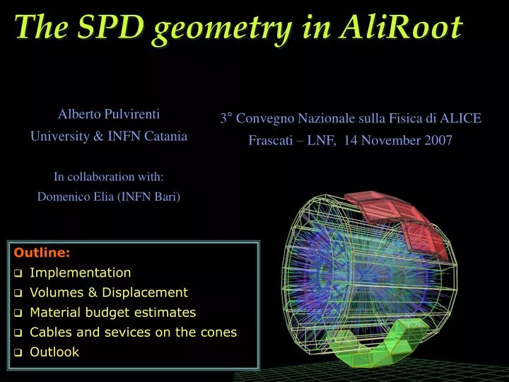
The SPD geometry in AliRoot 3° Convegno Nazionale sulla Fisica di ALICE Frascati – LNF, 14 November 2007 • Outline: • Implementation • Volumes & Displacement • Material budget estimates • Cables and sevices on the cones • Outlook Alberto Pulvirenti University & INFN Catania In collaboration with: Domenico Elia (INFN Bari)
Advantages of ROOT geometry modeling • Modeler independent from transport code (GEANT3, FLUKA, …) • geometry is implemented once for all transport engines • easy to be interfaced with the virtual “generic” simulation engine (TVirtualMC) • easy to swtich among different transport codes • Geometry built with ROOT classes • reusability for reconstruction • easy to implement (mis)alignment of modules
Components of a TGeo geometry • [TGeo]Medium: • a tracking medium (material + physical status) • [TGeo]Volume: • a block of material, which represents a part of the detector • a box which contains several sub-volumes, in order to be able to replicate a composite structure made of several parts • [TGeo]VolumeAssembly: • a “virtual” space with several volumes inside • useful to manage situations where a group of volumes can superimpose on another group of volumes
Implementation philosophy • Multi-level implementation: • all groups of volumes which are replicated many times in the whole detector are inserted into an “upper level” container • …which will be a TGeoVolume or TGeoVolumeAssembly depending on how its components are displaced in space • Advantages: • reduces the elements to be checked in case that corrections are needed • “logic” of the implementation is more easily readable and followable
Half-stave architecture Aluminum-polyimide multi-layer bus to connect the MCM and FE chip Aluminum-polyimide grounding foil (25 + 50 µm thick) with 11 windows to improve the thermal coupling • 2 Ladders consisting of: • p+n silicon sensor matrix 200 µm thick with 40960 pixels arranged in 256 rows and 160 columns • 5 FE chip Flip-chip bonded to the sensor through Sn-Pb bumps [single cell dimensions = 50 µm (r) x 425 µm (z)] Multi-chip module (MCM) to configure and read-out the half-stave
Implementation levels Sensor Chips Bumps Ladder Alignable Volumes “BASE” “Base” Resistors Pixel Bus ‘Box’ volume containing the grounding foil and the ladders. Pt1000 Capacitors Kapton Glues HALF STAVE Grounding Foil Al Grease MCM base Uppermost level Implemented as an assembly, to avoid some overlaps on the sector. MCM MCM Cover Chips inside MCM Pixel Bus Extender “Extenders” MCM Extender Thin cables which go from inside to outside the sensitive area of the SPD.
Stave architecture • 1 Stave = 1 “left” half-stave + 1 “right” half-stave “LEFT”-type half-stave “RIGHT”-type half-stave C - side A - side Example: couple of half-staves on the outer layer z x
Ladder • = 1 sensor + 5 chips + 32 bump-bondings one single container bump bondings implemented in “stripes” (1 x column) of • 0.042 mm width • 0.013 mm thickness guard ring around the sensor
Grounding foil • Complicated shape with holes inside • holes are filled with thermal grease • Cosisting in two layers (kapton & aluminum) • Small differences in size
Pixel bus Pt1000’s (one per chip) Big resistors and capacitors in correspondence of the end of each ladder
Half-stave assembly Needed some room for movement of ladders and half-staves to implement misalignment: this could cause an overlap of volumes. SOLUTION: reduce glue layer thickness to leave some “free space” around the ladder and between GF and support, without changing the spacing between components Pixel Bus Glue Glue Ladder Glue Glue Grounding Foil Glue Glue CARBON FIBER SUPPORT
Pixel bus & extenders (by R. Vernet) • Implemented as “folded” foils • Volumes must intrude in each other TGeoVolumeAssembly
MCM • Thin integrated circuit + Chips + Thick cover
Clips • Component on 3 over the 4 staves lying on layer 2
Placement on sector • Use reference points in the support placement planes
Tests (1)what is done on the way along implementation • Fix coding conventions • usually done before committing on CVS (by me or Massimo Masera) • Remove overlaps • the volumes must not overlap with each other, because this can cause the transport of particles to get confused and return meaningless data • a ROOT facility allows to check overlaps by sampling: • points are generated randomly in the volume of the complete geometry • for each point it is checked if it belongs to more than 1 volume • an alert is raised when this happens an overlap is present somewhere • Event generation in AliRoot with new geometry • check execution CPU time to detect anomalous increases due to slow geometry creation (e.g. due to a too large amount of volumes) • make sure that no run-time errors are raised
Tests (2)what will be done with dedicated tests • Check materials used for implementation • for objects present in the old geometry: • translate their definition in TGeo language (done by Ludovic Gaudichet) • for new objects only present in new geometry • when possible, reuse old definition (chips, silicon, …) • when not possible, a dedicated study is required to define new materials • Radiation Length maps • comparison between “old” and “new” geometries • comparison with computations from technical details
Calculated material budget (as implemented) 1.090 INNER LAYER OUTER LAYER 1.197 TH. SHIELD 0.530
Summary & outlook • The new TGeo package allows a definition of a detector geometry decoupled from transport code • ease switching among different transport codes • ease interacting with geometry also in reconstruction • Implementation of SPD has started since several months • Implemented part is almost equivalent to the actual geometry • work started for implementation of other components on cones • Testing of new geometry on the way • Preliminary tests being done for radiation length maps and event generation • Test on materials is going to start
X0 map: comparison with old geometry (very preliminary result) with “geantinos” New Layer 2 R = 6.5 7.5 cm Z (cm) Φ (deg) Old Z (cm) Φ (deg)
X0 map: comparison with old geometry (very preliminary result) with “geantinos”:difference Layer 2 R = 6.5 7.5 cm Z (cm) Φ (deg)
Cables and services on the cones: some estimates 1. Extenders: 12 per each (half-)sector: - 6 x pixel-bus - 6 x MCM X/Xo = 6*(0.11/285.7+0.14/14.3) = 6% X/Xo = 6*(0.10/285.7+0.10/14.3) = 4.4% 162o 18o 126o 54o 90o
Cables and services on the cones: some estimates 2. Optical patch-panels X/Xo = 4/27.0 = 14.8% 10 in total, 1 per each (half-)sector 90o 62o 115o 162o 18o 100mm yz 50mm Aluminium 50mm 4mm xy 50mm
Cables and services on the cones: some estimates 3. Plates holding the extenders X/Xo = 5/223.5 = 2.2% 10 in total, 1 per each (half-)sector at middle of the cone 200mm 50mm 30mm 50mm 2mm 5mm Carbon fiber xy xz
Cables and services on the cones: some estimates 4. Tubes for detector cooling X/Xo = 2/17.2 = 11.6% Flexible parts: 1mm Inox 6mm Central (rigid) part: may be assumed with same diameter but thinner walls (0.3mm)
Cables and services on the cones: some estimates 5. Other materials 4 of these capillars on the cone PHYNOX ducts 2.6mm xternal diameter 0.040mm thick walls X/X0 = 0.080/16.1 = 0.5% CARBON FIBER holding plate 300mm x 30mm 0.3mm thick X/X0 = 0.3/223.5 = 0.1% Cu/Ni (30/70) ducts 1.85mm external diameter 0.35mm thick walls 200mm length X/X0 = 0.7/14.3 = 4.9% Optical fibers (quartz) 18 per halh-sector: 9/125/900mm buffered fibers 1 fiber: X/X0 = 0.9/100 = 1.6% 18 fiber pockets X/Xo = 4.5/100 = 4.5% 4.5mm