Download
1 / 31
310 likes | 464 Views
Hardware Design of a 1 GHz Amplifier and Initial Comparison with SimRF Application Note. K. Wang, R. Ludwig, S. Bitar, S. Makarov Aug 21 , 2011. Outline . Lumped matching network Adding transmission line Layout generation Network analyzer measurement SimRF simulation.

E N D
Hardware Design of a 1 GHz Amplifier and Initial Comparison with SimRFApplication Note K. Wang, R. Ludwig, S. Bitar, S. Makarov Aug 21 , 2011
Outline • Lumped matching network • Adding transmission line • Layout generation • Network analyzer measurement • SimRF simulation
Lumped matching network Design uses active bias network and adds components with artwork instead of ideal components.
Lumped matching network Modeling of SMT inductor as RF choke
Lumped matching network • S-parameter extraction to test matching at input/output
Adding transmission line Specifying a 64 mil thick FR4 substrate and calculate TL parameters
Adding transmission line Adding transmission line to the input port We note mismatches at input and output
Adding transmission line Using tuning tool to match input/output Repeat the process until all the transmission line are added to the input and output port
Adding transmission line Final circuit schematic
Layout generation Use ADS Generate/Update layout to automatically generate layout
Layout generation The size of resistors, capacitors and inductors are set to 0805 size. Six layers are needed for the layout manufacture: 1) conductor, 2) ground plane, 3) top and 4) bottom solder masks, 5) via and 6) silkscreen.
Layout generation Final layout
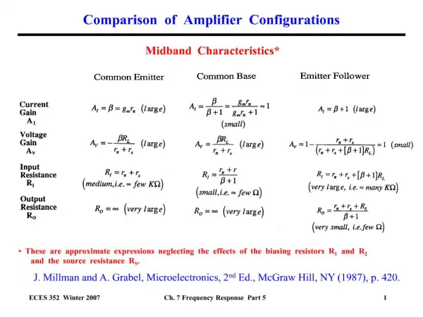
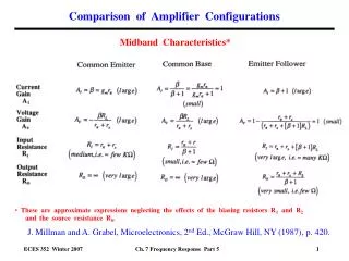
Network analyzer measurement Forward gain versus frequency S11 S22
Network analyzer measurement Gain compression at 1 GHz Gain compression at 1.3 GHz
SimRF simulation Based on NA measurements: G = 10.66 dB (at 1GHz) From Thus
SimRF simulation According to SimRF the power source equation is: For an input power of -36dBm:
SimRF simulation – 1GHz Input voltage 0.007 V
SimRF simulation – 1GHz Input voltage 0.14 V For an input power equal to -10 dBm, the input voltage is 0.14 V.
SimRF simulation – 1GHz Output voltage 0.46 V Gain = 10 * = 10.3 dB The gain has decreased a little as power increases.
SimRF simulation – 1GHz Input voltage 0.37 V For the input power equal to -1.62 dBm which is the input power for 1 dB gain compression, the input voltage is set to be 0.37 V.
SimRF simulation Output voltage = 0.944V Output voltage 0.944 V Gain = 10 * =8.14 dB
SimRF simulation – 1GHz Input voltage: 0.4472 V As the input power increases to 0 dBm, the input voltage is 0.4472 V.
SimRF simulation – 1GHz Output voltage: 0.963 V Gain = 10 * = 6.66 dB, the voltage becomes to stay the same.
SimRF simulation – 1.3GHz Input voltage: 0.14 V The input power is -10 dBm, and the voltage is 0.14V
SimRF simulation – 1.3GHz Output voltage 0.32 V Gain = 10 * = 7.18 dB
SimRF simulation – 1.3GHz Input voltage 0.4 V The input power is -1.1 dBm which is input power for 1 dB gain compression; the input voltage is 0.4 V.
SimRF simulation – 1.3GHz Output voltage 0.7 V Gain = 10 * = 4.86 dB
SimRF simulation – 1.3GHz Input voltage 0.5 V For input power of 1 dBm , the input voltage is 0.5 V.
SimRF simulation – 1.3GHz Output voltage 0.697 V Gain = 10 * = 2.88 dB, and the output voltage is same with the previous one.