Download
1 / 7
70 likes | 72 Views
The opto departation technique was used to transfer charge through the light photons from one mobile to other. The proximity of the mobile phones was very much important. The technique was introduced to reduce the wastage of time during charging and avoidance of unnecessaryshut down of mobile phones. The simulation was done in multisim and the hardware implementation was done using a opto coupler and a photo diode. The results were obtained in multisim. G. Naveen Balaji | S. Chenthur Pandian | S. Giridharan | S. Shobana | J. Gayathri "Dynamic and Non-Linear Charge Transfer through Opto-Deportation by Photovoltaic Cell" Published in International Journal of Trend in Scientific Research and Development (ijtsrd), ISSN: 2456-6470, Volume-1 | Issue-5 , August 2017, URL: https://www.ijtsrd.com/papers/ijtsrd2329.pdf Paper URL: http://www.ijtsrd.com/engineering/electronics-and-communication-engineering/2329/dynamic-and-non-linear-charge-transfer-through-opto-deportation-by-photovoltaic-cell/g-naveen-balaji<br>

E N D
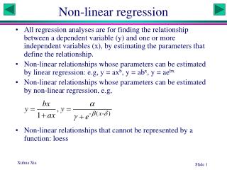
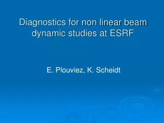
International Journal of Trend in Scientific Research and Development (IJTSRD) UGC Approved International Open Access Journal ISSN No: 2456 - 6470 | www.ijtsrd.com | Volume - 1 | Issue – 5 Dynamic and Non-Linear Charge Transfer Through Opto-Deportation by Photovoltaic Cell G. Naveen Balaji Assistant Professor, Department of ECE, SNS College of Technology Coimbatore, India S. Chenthur Pandian Principal & Director, Department of EEE, SNS College of Technology, Coimbatore, India S. Giridharan UG Student, Department of ECE SNS College of Technology, Coimbatore, India S. Shobana J. Gayathri UG Student, Department of ECE SNS College of Technology, Coimbatore, India ABSTRACT UG Student, Department of ECE SNS College of Technology, Coimbatore, India The opto departation technique was used to transfer charge through the light photons from one mobile to other. The proximity of the mobile phones was very much important. The technique was introduced to reduce the wastage of time during charging and avoidance of unnecessary shut down of mobile phones. The simulation was done in multisim and the hardware implementation was done using a opto coupler and a photo diode. The results were obtained in multisim. Keywords: Opto coupler, Charging, Mobile device, Photodiode phototransistor, phototriac, photodarlington circuit or a photo SCR. I. INTRODUCTION Fig 1: Different opto coupler circuits An opto coupler also called opto isolator is an electronic device that transfers an electrical signal or voltage from one part of a circuit to another where the two circuits are electrically isolated from each other. The opto coupler circuit consists of an infrared emitting led that is optically in line with a light sensitive silicon semiconductor. The light sensitive silicon semiconductor may be a photodiode, Fig 2: Opto coupler circuit @ IJTSRD | Available Online @ www.ijtsrd.com | Volume – 1 | Issue – 5 | July-Aug 2017 Page: 486
International Journal of Trend in Scientific Research and Development (IJTSRD) ISSN: 2456-6470 II. A. LIGHT EMITTING DIODE (LED) OTHER TYPES A “Light Emitting Diode” or LED is a special type of PN junction diode, made from a very thin layer of fairly heavily doped semiconductor material. ➢Gallium Arsenide (GaAs) - infra-red ➢ Gallium Arsenide Phosphide (GaAsP) - red to infra-red, orange ➢ Aluminium Gallium Arsenide Phosphide (AlGaAsP) - high-brightness red, orange- red, orange, and yellow ➢Gallium Phosphide (GaP) - red, yellow and green ➢ Aluminium Gallium Phosphide (AlGaP) - green ➢ Gallium Nitride (GaN) - green, emerald green ➢ Gallium Indium Nitride (GaInN) - near ultraviolet, bluish-green and blue ➢ Silicon Carbide (SiC) - blue as a substrate ➢ Zinc Selenide (ZnSe) - blue ➢ Aluminium Gallium Nitride (AlGaN) – ultraviolet Fig 3: Light Emitting Diode (LED) III. WORKING When the diode is forward biased, electrons from the semiconductors conduction band recombine with holes from the valence band releasing sufficient energy to produce photons monochromatic (single colour) of light. Because of this thin layer a reasonable number of these photons can leave the junction and radiate away producing a coloured light output. when it is operated in a forward biased direction Light semiconductor devices that convert electrical energy into light energy. which emit a Emitting Diodes are B. APPLICATIONS AUTOMOTIVE: In the interior of automobile that includes indicator lights on dash board, audio status lights and exterior of automobile includes third brake light , left and right rear Lamps etc DISPLAY SCREEN: The LED screens has become the new medium for advertising and information. It offers advantages such as high brightness, high reliability, low energy consumption, long service life, low maintenance cost etc. LED displays have been widely adapted in various fields. ELECTRONIC EQUIPMENT: due to attributes such as low power consumption, small size and long life, LED’S have been preferred in light sources on various electronic equipment such as warning light, indicators etc. GENERAL LIGHTINING: LED’S are being used in advertising billboards, illumination of commercial building exteriors, landmark buildings, bridges, roads etc. A.TYPES TYPE 1: Aluminium Gallium Arsenide (AlGaAs) led’s are mainly used in the opto coupler product families that includes digital opto couplers, isolation amplifiers, gate drivers etc. These led’s provide the highest light output power among all the types. TYPE 2: Aluminium Gallium Phosphate (AlGaP) belongs to avago’s opto coupler family that handles high speed digital signals and low power digital opto couplers .This of led has a performance which lies between type 1 and type 3 led. It has an wavelength of about 550-570nm. It is operated at 3.5volt. TYPE 3: Gallium Arsenide Phosphorus (GaAsP). These led’s have wide applications in analog opto coupler, intelligent power management many. Type 3 led’s are the most mature but have the lowest light output power. It is operated at two different wavelength one at 630-660nm producing red colour operating at 1.8 volt and the other having a wavelength of 605-620nm producing amber colour operating at 2.0 volt. @ IJTSRD | Available Online @ www.ijtsrd.com | Volume – 1 | Issue – 5 | July-Aug 2017 Page: 487
International Journal of Trend in Scientific Research and Development (IJTSRD) ISSN: 2456-6470 IV. PHOTO DIODE ➢PN junction photo diode ➢Avalanche photo diode ➢PIN photo diode Normal PN junction photo diode is used in low frequency and low sensitive applications. When high frequency of operation and high sensitivity is needed avalanche photo diode or PIN photo diodes are used. E. Principle of operation photodiode: When a PN junction is illuminated with light, it ionizes covalent bonds and new hole, electron pairs are generated in excess of thermally generated pairs. If the photo generation occurs at a distance of the diffusion length order or less depletion layer the photo generated electron hole pairs are swept across by the applied reverse bias field. This mode of operation of photo diode is called photo conductive mode. The photo current varies almost linearly with incident light flux or optical power. The mode of operation of photo diode is called photo conductive diode. The current equation of a Photo diode is given as I = IS+ IO*(1-eV/ (η*Vt)) Whereηis 1 for Ge and 2 for Si, Vt is voltage equivalent of temperature, Is the short circuit current proportional to light intensity, Io is reverse saturation current of diode, V is positive for forward bias and negative for reverse bias. Photo current is diffusion current. F. PIN PHOTODIODE PIN photodiode (Fig 4.1) is a kind of photo detector, it can convert optical signals into electrical signals.Thereare three regions in this type of diode. There is a p-region an intrinsic region and an n- region.Thep-region and n-region are comparatively heavily doped than the p-region and n-region of usual p-n diodes. The width of the intrinsic region should be larger than the space charge width of a normal p-n junction. The PIN photodiode operates with an applied reverse bias voltage and when the reverse bias is applied, the space charge region must cover the intrinsic region completely. Electron hole pairs are generated in the space charge region by photon absorption. Photo means light and diode means a device consisting of two electrodes. A photo diode is a light sensitive electronic device capable of converting light into a voltage or current signal. It works on the principle of photo generation. A. Symbol of Photo Diode Photo diode has two terminals anode and cathode with the arrows indicating that the light rays falling on photo diode reflecting its significance as a photo detector PN junction Fig 4: Photo diode B. Physical Structure of photo diode A normal PN junction photo diode (Fig 4.1) is made by sandwiching a P type semiconductor into N type semiconductor. All the sides of PN junction diode is enclosed in metallic case or painted black except for one side on which radiation is allowed to fall. C. Modes of operation of Photo diode A photo sensitive diode can be operated mainly in two modes ➢Photo conductive mode ➢Photo voltaic mode The photo diodes used as photo detectors are optimized (in the physical construction of the device itself) to have fast response times whereas the photo diodes used in electrical energy generation are optimized to have high efficiency of energy conversion. The photo detectors are operated in photo conductive mode. Solar cells are operated in Photo voltaic mode. D. Types of photo diodes There are mainly three types of photo diodes @ IJTSRD | Available Online @ www.ijtsrd.com | Volume – 1 | Issue – 5 | July-Aug 2017 Page: 488
International Journal of Trend in Scientific Research and Development (IJTSRD) ISSN: 2456-6470 H. APPLICATIONS ➢PIN diode, find applications in audio CD players, DVD players as well as computer CD drives. In addition to this they are used in optical communication systems. ➢PIN photodiode are also used as nuclear radiation detectors. There are several types of nuclear radiation. The radiation may be in the form of high energy charged or uncharged particles, or it may also be electromagnetic radiation. ➢The PIN diode can also be used as an RF switch. ➢Another useful application of the PIN diode is for use in RF protection circuits V. VALANCHE PHOTO DIODE Fig 5: Pin photo diode G. CHARACTERISTICS PIN diode characteristics include the following: ➢High breakdown voltage: The wide depletion layer provided by the intrinsic layer ensures that PIN diodes have a high reverse breakdown characteristic. ➢Low capacitance: Again the intrinsic layer increases the depletion region width. As the capacitance of a capacitor reduces with increasing separation, this means that a PIN diode will have a lower capacitance as the depletion region will be wider than a conventional diode. This PIN diode characteristic can have significant advantages in a number of RF applications - for example when a PIN diode is used as an RF switch. ➢Carrier storage: Carrier storage gives a most useful PIN diode characteristic. For small signals at high frequencies the stored carriers within the intrinsic layer are not completely swept by the RF signal or recombination. At these frequencies there is no rectification or distortion and the PIN diode characteristic is that of a linear resistor which introduces no distortion or rectification. The PIN diode resistance is governed by the DC bias applied. In this way it is possible to use the device as an effective RF switch or variable resistor for an attenuator producing far less distortion than ordinary PN junction diodes. ➢Sensitive Potodetection: The sensitive area of a photodiode is the depletion region. Light striking the crystal lattice can release holes and electrons which are drawn away out of the depletion region by the reverse bias on the diode. By having a larger depletion region - as in the case of a PIN diode - the volume for light reception is increased. This makes PIN diodes ideal for use as photo detectors. The avalanche photodiode possesses a similar structure to that of the PIN or PN photodiode. The main difference of the avalanche photodiode operates under a slightly different scenario to that of the more standard photodiodes. It operates under a high reverse bias condition to enable avalanche multiplication of the holes and electrons created by the initial hole electron pairs created by the photon / light impact. The avalanche action enables the gain of the diode to be increased many times, providing a much greater level of sensitivity. A.CHARACTERISTICS Avalanche Photodiodes (APDs) are high sensitivity, high speed semi-conductor "light" sensors. Compared to regular PIN construction photodiodes, APDs, have an internal region where electron multiplication occurs, by application of an external reverse voltage, and the resultant "gain" in the output signal means that low light levels can be measured at high speed. B.ADVANTAGE The main advantages of the avalanche photodiode include: ➢Greater level of sensitivity ➢Avalanche photodiode produces a much higher level of noise than a p-n photodiode ➢Avalanche process means that the output is not linear C. TYPES OF EXCITATION There can be two types of photo excitations they are @ IJTSRD | Available Online @ www.ijtsrd.com | Volume – 1 | Issue – 5 | July-Aug 2017 Page: 489
International Journal of Trend in Scientific Research and Development (IJTSRD) ISSN: 2456-6470 E. Applications of photo diodes ▪Photo diodes are used as photo detectors ▪Photo diodes are used in providing electric isolation using a special circuitry called as Opto couplers. Opto coupler is an electronic component which is used in coupling optically the two isolated circuits by using light. The two circuits are optically coupled but electrically isolated. It is a combination of light emitting diode and photo diode (or) avalanche diode (or) photo transistor. Opto couplers are faster than the conventional devices. ▪They are used in consumer electronics ▪ They are used in cameras as photo sensors, Slotted optical switch, in scintillates e.t.c F. WORKING OF OPTOCOUPLER When a forward bias voltage is applied to the input terminal of led(positive to the anode) an input current flows through the led circuit. The current produces the infrared light emission at its wavelength of 900nm that impinges on photo sensitive silicon conductor i.e. photo transistor making the transistor to work on the reverse condition .with the light impinging on the silicon transistor its photo voltaic characteristics will create photo current to flow through the transistor. With a load resistor connected to the output terminal, the photo current develops a voltage across the resistor. A load such as an led, relay etc. are connected to check the voltage flow. I. APPLICATIONS At present opto coupler’s are used in the field of telecommunication for noiseless transmission. There is also specific opto telecommunication where the data transmission rate is about Gb/sec. The other applications of opto coupler include AC and DC power control, signal isolation, pc communication. II. PROPOSED APPLICATION In our proposed application we make use of opto coupler device in mobile phone so as to transfer charge from one mobile to the other. 1. Intrinsic excitations 2. Extrinsic excitations Intrinsic excitations occur when an electron in valence band is excited by a high energy photon to conduction band. Alternatively a photon may excite an electron in donor level to conduction band or a valence band electron may go into acceptor state. Such excitations are termed as extrinsic excitations. The minimum energy of light required for photo generation due to intrinsic excitation is the forbidden gap energy EG. The wavelength associated with this critical energy is known as critical wavelength. λ = 1.24/ EG(in eV) Photons with wavelength greater than critical wavelength cannot generate new charge carrier pairs. D. VI Characteristics of Photo Diode The VI characteristic of a photo diode is shown in the figure 6. Fig 6: Photo diode IV characteristics coupler used in A photo diode is always operated in reverse bias mode. From the photo diode characteristics it is seen clearly that the photo current is almost independent of applied reverse bias voltage. For zero luminance the photo current is almost zero except for small dark current. It is of the order of NANO amperes. As optical power increases the photo current also increases linearly. The maximum photo current is limited by the power dissipation of the photo diode. @ IJTSRD | Available Online @ www.ijtsrd.com | Volume – 1 | Issue – 5 | July-Aug 2017 Page: 490
International Journal of Trend in Scientific Research and Development (IJTSRD) ISSN: 2456-6470 III. BLOCK DIAGRAM A. Multisim Texas National Instruments in Jan 12, 2010 has introduced Multisim 11, the latest version of its circuit simulation software, with specialized editions for both hands-on learning and professional circuit design. The easy-to-use Multisim software delivers a graphical approach that abstracts the complexities of traditional circuit simulation, helping educators, students and engineers employ advanced technology. Fig 7: Block disgram of opto deportation circuit analysis IV. WORKING We use mobile battery as the source for the device .The flash light in the mobile act as the led at the transmitting end. On the other hand a mobile is fixed with light sensitive photo transistor which acts as the receiver. When we are in need to transfer charge the flash light in the mobileat the transmitting end is made ON. The light emitted from flash light is sensed by the photo transistor on the other end therefore at the receiver a photovoltaic current flows through the circuit which is in turn connected to the battery. In such away charge transformation is achieved Fig (7.1) .The main factor that has to be considered is that the photo transistor used at the receiver end must be high sensitive to light so as to reduce the delay of transformation. Fig 9: Simulation result in Multisim VI. ADVANTAGES The academic edition of Multisim 11 incorporates specialized teaching features and is complemented by circuit’s textbooks and courseware. This integrated system helps educators engage students and reinforce circuit theory with an interactive, hands-on approach to investigating circuit behavior. ➢Simplify digital circuits teaching by exporting raw VHDL from a programmable logic device (PLD) schematic ➢Guide hands-on electronics experiments with new educator-requested AC single-frequency analysis ➢Correlate simulated measurements by integrating Electronic Laboratory Virtual Instrumentation Suite (NI ELVIS) educational platform VII. CONCLUSION data with real-world with the NI prototyping Fig 8: Expected result By using this technique low cost power transfer can be achieved. Since it is wireless power transfer low number of resources is utilized. V. SIMULATION RESULT ANALYSIS The simulation result of our proposed circuit has been verified using the multisim software. @ IJTSRD | Available Online @ www.ijtsrd.com | Volume – 1 | Issue – 5 | July-Aug 2017 Page: 491
International Journal of Trend in Scientific Research and Development (IJTSRD) ISSN: 2456-6470 [5] H.M. Elqudaby, G.G. Mohamed, G.M.G. El- Din, Spectrochim. Acta Part A., 129 (2014) 84. [6] H.H. Eldaroti, S.A. Gadir, M.S. Refat, A.M.A. Adam, Spectrochim. Acta Part A, 115 (2013) 309. ACKNOWLEDGMENT This work is supported in part by a grant from the SNS College of Technology. This topic was suggested in the seed money proposals. Later this work was carried out by the juniors of the same. REFERENCES [1] G. Smith, D.E. Lynch, K.A. Byriel, C.H.L. Kennard, J. Chem. Crystallogr. 27 (1997) 307. [2] M.S. Refat, O.B. Ibrahim, H.A. Saad, A.M.A. Adam, J. Mol. Struct., 1064 (2014) 58. [3] H.H. Eldaroti, S.A. Gadir, M.S. Refat, A.M.A. Adam, J. Pharma. Anal., 4(2) (2014) 81. [4] A.A. El-Habeeb, F.A. Al-Saif, M.S. Refat, Spectrochim. Acta Part A, 123 (2014) 455. @ IJTSRD | Available Online @ www.ijtsrd.com | Volume – 1 | Issue – 5 | July-Aug 2017 Page: 492