Download
1 / 28
280 likes | 285 Views
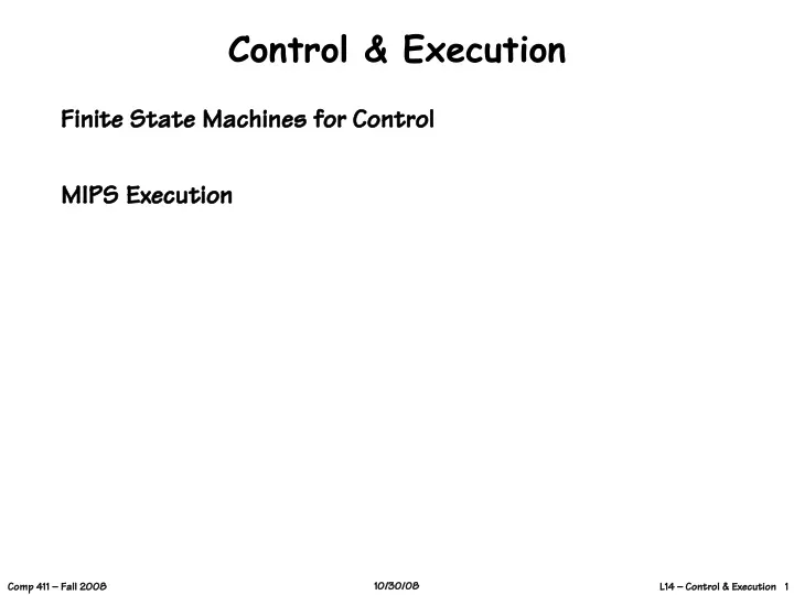
Control & Execution. Finite State Machines for Control MIPS Execution. Synchronous Systems. Combinational logic. Flipflop. Flipflop. data. trailing edge. Clock. leading edge. On the leading edge of the clock, the input of a flipflop is transferred to the output and held.

E N D
Control & Execution • Finite State Machines for Control • MIPS Execution
Synchronous Systems Combinational logic Flipflop Flipflop data trailing edge Clock leading edge On the leading edge of the clock, the input of a flipflop is transferred to the output and held. We must be sure the output of the combinational logic has settled before the next leading clock edge.
Asynchronous Systems Combinational logic Latch Latch data valid No clock! The data carries a “valid” signal along with it System goes at greatest possible speed. Only “computes” when necessary. Everything we look at in this class will be synchronous Asynchronous is my specialization!
Fetching Sequential Instructions + 4 P C Read Address Instruction flipflop Instruction Memory How about branch?
Datapath for R-type Instructions ALU Operation 3 5 Inst Bits 25-21 Read Reg. 1 (rs) 32 data 1 5 Inst Bits 20-16 Read Reg. 2 (rt) 5 Inst Bits 15-11 Write Reg. (rd) 32 data 2 32 Write Data RegWrite
Fun with MUXes Remember the MUX? Select 0 In 3 Select 1 In 2 Out Select 0 In 1 This will route 1 of 4different 1 bit valuesto the output. In 0
MUX Blocks Select Select 2 1 0 3 0 1 8 In Out 2 Input 3 Out 4 5 6 7 The select signal determines which of the inputs is connectedto the output
Inside there is a 32 way MUX per bit Read Reg 1 5 Register 0 32 to1 MUX Register 1 Register 2 Data 1 Register 3 Register 4 Register ... LOT’S OF CONNECTIONS! Register 30 Register 31 And this is just one port! Remember, there’s data1 and data2 coming out of the register file! For EACH bit in the 32 bit register
Our Register File has 3 ports This is one reason we have only a small number of registers 2 Read Ports What’s another reason? 5 Inst Bits 25-21 Read Reg. 1 32 data 1 5 Inst Bits 20-16 Read Reg. 2 5 Inst Bits 15-11 Write Reg. 32 data 2 32 Write Data REALLY LOTS OF CONNECTIONS! 1 Write Port RegWrite
Implementing Logical Functions Suppose we want to map M input bits to N output bits For example, we need to take the OPCODE field from the instruction and determine what OPERATION to send to the ALU. OPCODE bitsfrom instruction Map to ALU op ALU Operation (8 different ops) 3 32 32
We can get 1 bit out with a MUX Put the INPUT HERE Wire these to HIGH or LOW depending on the value you want OUT for that INPUT Select 2 1 0 0 1 2 Input 3 Out For example, 3 input AND has INPUT7 wired HIGH and all the others wired LOW. 4 5 6 7
Or use a ROM Read-Only Memory M-bit Address N-bit Result
Or use sum-of-products OR layer AND layer M-bit Input Product Terms N-bit Output Think of the SUM of PRODUCTS form. The AND layer generates the products of various input bits The OR layer combines the products into various outputs You could also use two NAND layers instead Could be implemented using Boolean gates, or also using a “programmable logic array” (PLA) [similar to a PROM, but both the AND and the OR parts are programmable].
Finite State Machines • A set of STATES • A set of INPUTS • A set of OUTPUTS • A function to map the STATE and the INPUT into the next STATE and an OUTPUT Remember automata?
Traffic Light Controller G E/W R N/S Y E/W R N/S R E/W G N/S R E/W Y N/S
Implementing an FSM Function (comb. logic) Outputs Inputs State(flipflops) Clock
FSM Example: Recognizing Numbers • Recognize the regular expression for floating point numbers • [ \t]* [-+]?[0-9]*(. [0-9]*)? (e[-+]?[0–9]+)? • Examples: • +123.456e23 • .456 • 1.5e-10 • -123 “a” matches itself “[abc]” matches one of a, b, or c “[a-z]” matches one of a, b, c, d, ..., x, y, or z “0*” matches zero or more 0’s (“”, “0”, “00”, “0000”) “Z?” matches zero or 1 Z’s
FSM Diagram ‘ ’ start ‘.’ done ‘ ’ ‘+’ ‘-’ ‘0’ – ‘9’ sign ‘0’ – ‘9’ ‘ ’ whole ‘ ’ ‘.’ ‘.’ ‘0’ – ‘9’ frac ‘0’ – ‘9’ ‘e’ exp ‘e’
FSM Table IN : STATE NEW STATE ‘ ’ : start start ‘0’ | ‘1’ | ... | ‘9’ : start whole ‘+’ | ‘-’ : start sign ‘.’ : start frac ‘0’ | ‘1’ | ... | ‘9’ : sign whole ‘.’ : sign frac ‘0’ | ‘1’ | ... | ‘9’ : whole whole ‘.’ : whole frac ‘ ’ : whole done ‘e’ : whole exp ‘e’ : frac exp ‘0’ | ‘1’ | ... | ‘9’ : frac frac ‘ ’ : frac done ‘0’ | ‘1’ | ... | ‘9’ : exp exp ‘ ’ : exp done STATE ASSIGNMENTS start = 0 = 000 sign = 1 = 001 whole = 2 = 010 frac = 3 = 011 exp = 4 = 100 done = 5 = 101 error = 6 = 110
FSM Implementation ROM or PLAor comb. logic error 8 char in ok state 3 3 • Our PLA has: • 11 inputs • 5 outputs
FSM Summary • With JUST a register and some logic, we can implement complicated sequential functions like recognizing a FP number. • This is useful in its own right for compilers, input routines, etc. • The reason we’re looking at it here is to see how designers implement the complicated sequences of events required to implement instructions • Think of the OP-CODE as playing the role of the input character in the recognizer. The character AND the state determine the next state (and action).
Five Execution Steps • 1. Instruction Fetch • 2. Instruction Decode and Register Fetch • 3. Execution, Memory Address Computation, or Branch Completion • 4. Memory Access or R-type instruction completion • 5. Memory Read Completion INSTRUCTIONS TAKE FROM 3 - 5 CYCLES! • An FSM looks at the op-code to determine how many...
Step 1: Instruction Fetch • Use PC to get instruction and put it in the Instruction Register. • Increment the PC by 4 and put the result back in the PC. • Can be described succinctly using RTL "Register-Transfer Language" IR = Memory[PC]; IR is “Instruction Register” PC = PC + 4;
Step 2: Instruction Decode and Register Fetch • Read registers rs and rt in case we need them • Compute the branch address in case the instruction is a branch • RTL:A = Reg[IR[25-21]]; B = Reg[IR[20-16]];ALUOut = PC + (sign-extend(IR[15-0]) << 2); • We aren't setting any control lines based on the instruction type (we are busy "decoding" it in our control logic)
Step 3 (instruction dependent) • ALU is performing one of three functions, based on instruction type • Memory Reference:ALUOut = A + sign-extend(IR[15-0]); • R-type:ALUOut = A op B; • Branch:if (A==B) PC = ALUOut;
Step 4 (R-type or memory-access) • Loads and stores access memory • MDR = Memory[ALUOut]; MDR is Memory Data Register or Memory[ALUOut] = B; • R-type instructions finish Reg[IR[15-11]] = ALUOut;
Step 5 Memory Read Completion • Reg[IR[20-16]]= MDR;