Download
1 / 1
10 likes | 103 Views
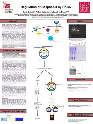
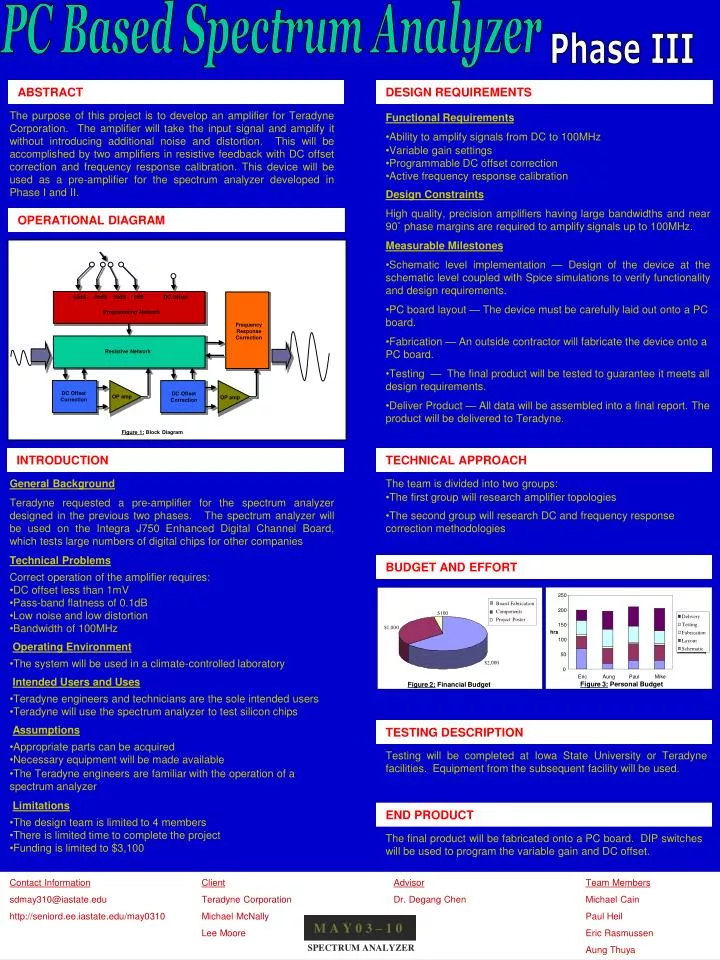
PC Based Spectrum Analyzer. 60dB 40dB 20dB 6dB . DC Offset. Programming Network. Frequency Response Correction. Resistive Network. DC Offset Correction. DC Offset Correction. OP amp. OP amp. Figure 1: Block Diagram. Board Fabrication. Components. $100. Project Poster.

E N D
PC Based Spectrum Analyzer 60dB 40dB 20dB 6dB DC Offset Programming Network Frequency Response Correction Resistive Network DC Offset Correction DC Offset Correction OP amp OP amp Figure 1: Block Diagram Board Fabrication Components $100 Project Poster $1,000 $2,000 Figure 2: Financial Budget Phase III ABSTRACT DESIGN REQUIREMENTS The purpose of this project is to develop an amplifier for Teradyne Corporation. The amplifier will take the input signal and amplify it without introducing additional noise and distortion. This will be accomplished by two amplifiers in resistive feedback with DC offset correction and frequency response calibration. This device will be used as a pre-amplifier for the spectrum analyzer developed in Phase I and II. • Functional Requirements • Ability to amplify signals from DC to 100MHz • Variable gain settings • Programmable DC offset correction • Active frequency response calibration • Design Constraints • High quality, precision amplifiers having large bandwidths and near 90˚ phase margins are required to amplify signals up to 100MHz. • Measurable Milestones • Schematic level implementation — Design of the device at the schematic level coupled with Spice simulations to verify functionality and design requirements. • PC board layout — The device must be carefully laid out onto a PC board. • Fabrication — An outside contractor will fabricate the device onto a PC board. • Testing — The final product will be tested to guarantee it meets all design requirements. • Deliver Product — All data will be assembled into a final report. The product will be delivered to Teradyne. OPERATIONAL DIAGRAM INTRODUCTION TECHNICAL APPROACH • General Background • Teradyne requested a pre-amplifier for the spectrum analyzer designed in the previous two phases. The spectrum analyzer will be used on the Integra J750 Enhanced Digital Channel Board, which tests large numbers of digital chips for other companies • Technical Problems • Correct operation of the amplifier requires: • DC offset less than 1mV • Pass-band flatness of 0.1dB • Low noise and low distortion • Bandwidth of 100MHz • Operating Environment • The system will be used in a climate-controlled laboratory • Intended Users and Uses • Teradyne engineers and technicians are the sole intended users • Teradyne will use the spectrum analyzer to test silicon chips • Assumptions • Appropriate parts can be acquired • Necessary equipment will be made available • The Teradyne engineers are familiar with the operation of a spectrum analyzer • Limitations • The design team is limited to 4 members • There is limited time to complete the project • Funding is limited to $3,100 • The team is divided into two groups: • The first group will research amplifier topologies • The second group will research DC and frequency response correction methodologies BUDGET AND EFFORT 250 200 Delivery Testing 150 hrs Fabrication 100 Layout Schematic 50 0 Eric Aung Paul Mike Figure 3: Personal Budget TESTING DESCRIPTION Testing will be completed at Iowa State University or Teradyne facilities. Equipment from the subsequent facility will be used. END PRODUCT The final product will be fabricated onto a PC board. DIP switches will be used to program the variable gain and DC offset. Contact InformationClientAdvisorTeam Members sdmay310@iastate.edu Teradyne Corporation Dr. Degang Chen Michael Cain http://seniord.ee.iastate.edu/may0310 Michael McNally Paul Heil Lee Moore Eric Rasmussen Aung Thuya M A Y 0 3 – 1 0 SPECTRUM ANALYZER