Download
1 / 25
250 likes | 455 Views
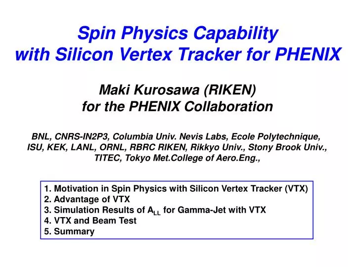
Spin Physics Capability with Silicon Vertex Tracker for PHENIX Maki Kurosawa (RIKEN) for the PHENIX Collaboration BNL, CNRS-IN2P3, Columbia Univ. Nevis Labs, Ecole Polytechnique, ISU, KEK, LANL, ORNL, RBRC RIKEN, Rikkyo Univ., Stony Brook Univ., TITEC, Tokyo Met.College of Aero.Eng.,.

E N D
Spin Physics Capability with Silicon Vertex Tracker for PHENIX Maki Kurosawa (RIKEN) for the PHENIX Collaboration BNL, CNRS-IN2P3, Columbia Univ. Nevis Labs, Ecole Polytechnique, ISU, KEK, LANL, ORNL, RBRC RIKEN, Rikkyo Univ., Stony Brook Univ., TITEC, Tokyo Met.College of Aero.Eng., 1. Motivation in Spin Physics with Silicon Vertex Tracker (VTX) 2. Advantage of VTX 3. Simulation Results of ALL for Gamma-Jet with VTX 4. VTX and Beam Test 5. Summary
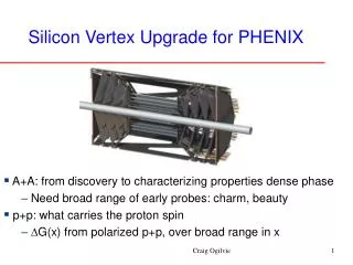
Motivation in Spin Program with VTX Direct g (pT(g), hg) Large Acceptance (hjet) Jet VTX detector satisfied these requirements • Gluon spin structure of the nucleon • Gluon polarization G/G with charm, beauty. • x dependence of G/G with -jet correlations. • Requirements for detector • Heavy flavor tagging and beauty and charm separation : Good vertex resolution • x reconstruction with recoil jet (pT(g), hg, hjet) : Large solid angle coverage
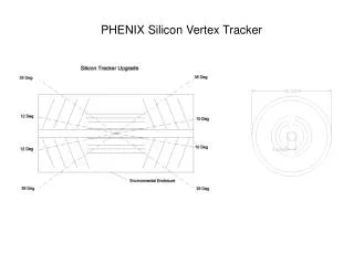
VTX Detector • Four-Layer Barrel Detector • Pixel Sensor (Inner 2 Layers)(50 x 425 mm2) • required for high occupancy • Strip Sensor(Outer 2 Layers) (80 x 1000 mm2) • Good DCA resolution • sDCA~ 50 mm • Large Acceptance • |h| < 1.2, 2p for f |h| < 1.2 2p for f Pixel Layers r=5.0cm Dz=±10cm r=2.5cm Dz=±10cm Strip Layers r=10cm Dz=±16cm r=14cm Dz=±19cm
Advantage with VTX Detector (Heavy Flavor) Simulation Background c quark b quark charm and beauty separation with difference of their life time e Life time (ct) D0 : 125 mm B0 : 464 mm DCA D p p B By simultaneous fitting the DCA distribution with the expected shapes, charm and beauty are separated. e Subtraction of background DCA (mm) pT (GeV/c)
Advantage with VTX Detector (g-jet Measurement) |h| < 0.35 Direct g PHENIX |h| < 0.35 jet Jet |h| < 0.35 |h| < 1.2 vertex |hjet| < 1.2 VTX can improve xgluon determination
Gamma - Jet with VTX Jet axis was reconstructed with VTX by using PYTHIA simulation xg is calculated by the kinematical reconstruction with jet axis information Simple Cone Algorithm (corn radius < 0.5 in eta-phi space) was used. Without VTX With VTX w/o jet information w/ jet reconstruction With jet axis reconstruction, improvement of the xg reconstruction.
Gamma - Jet with VTX Center of mass energy Integrated Luminosity ALL distribution as function of xg PYTHIA Simulation Dg = g GRSV_std L = 300 pb -1 P = 0.7 Dg = -g
VTX Detector ( Pixel ) Silicon Sensor 56.72mm 13.92mm • - Hybrid Pixel Sensor - • Technology developed by ALICE. • Bump-bonding between R/O chip • and sensor.. bump bond R/O Chip Sensor R/O chip wafer • Pixel R/O Chip • 425mm(z) x 50mm(f)/pixel • 32(z) x 256(f) = 8192 pixels • Active area is 12.8 x 13.6 mm2 • 150 mm thickness • Operation at 10 MHz • Power consumption is 1W/chip 50mm 256 row 425mm 32 column Sensor wafer • Pixel Sensor • Same pixel size of R/O chip • 200 mm thickness
VTX Detector ( Strip ) • - Strip Sensor - • Single-sided sensor with 2-D position sensitivity • Charge sharing by 2 spirals in one pixel • Sensor (Hamamatsu) 3.5 x 6.4 cm2 625 mm thickness • Pixels : 384 x 30 x 2 = 23k • Strips : 384 x 2 x 2 = 1.5k Sensor elements: Finely segmented detector with 80 µm 1 mm, pixels. Each pixel region has two metal strips and collect charge from sensor. 128 ch/chip 8 bit ADC
VTX Detector 2 pixel bus 4 hybrid sensor cooling support pixel ladders • Pixel detector = Inner 2 layers of VTX • 1st layer: 10 pixel ladders= 40 hybrid sensor • 2nd layer: 20 pixel ladders = 80 hybrid sensor VTX will be installed into PHENIX in 2010 stripmodule strip ladders 5 or 6 strip module cooling support • Strip detector = Outer 2 layers of VTX • 3rd layer: 16strip ladders= 80 strip modules • 4th layer: 24strip ladders = 144 strip modules 10
FNAL Beam Test STRIP 3 LAYERS scintillator S1 PIXEL 3 LAYERS S4 S2 S3 Beam SPIRO 1 SPIRO 2 SPIRO 3 RCC 1 RCC 2 RCC 3 optical cable FEM FEM PHENIX DAQ DAQ To confirm functionality of silicon detector and DAQ system, full chain test had been performed by using beam at FNAL (MT984) • 20-26 Aug MTest beam line • 120GeV/c proton beam • 10 x 10 mm2 beam-focus • 3 pixel detectors and 3 strip detectors
We perform beam test at FNAL in order to check the functionality of silicon pixel ladder and confirm DAQ system works properly PIXEL 3 LAYER STRIP 3 LAYER beam
FNAL Beam Test Layer 1 Layer 2 Layer 3 row col Event Display Intrinsic Resolution for row (f) direction chip1 chip2 chip3 chip4 Beam Preliminary row [mm] Clear tracking
FNAL Beam Test Event Display Residual Distribution Beam Layer 3 RMS=0.91 Layer 5 RMS=0.45 ( =36 mm ) RMS=0.90 Layer 6 Red circle : clusters with ADC > 3 sigma
Summary • Silicon Vertex Tracker (VTX) can enhance physics capability of the • PHENIX detector. • PYTHIA simulation was performed under the condition of • and . • Improvement for x reconstruction with gamma-jet production. • Estimation of ALL as a function of xg. • FNAL beam test was performed to confirm the functionality of detector • and DAQ system. The system worked properly. • Preparation for mass production is under way. • VTX detector will be installed into PHENIX in 2010.
Advantage with VTX Detector Baseline detector VTX barrel upgrade Gluon polarization will be measured by prompt photon (g + jet) single electron (charm and bottom tagging) VTX extend the x-range.
DCA Resolution DCA resolution is dominated most inner two layers. pT (GeV/c)
Occupancy (PISA Simulation) • Occupancy of the each layers in the central Au-Au collisions • Pixel Layer • N_hits : hit counts on each layer • N_allpix : all pixel numbers on each layer ( 32 x 256 x 4 x 4x 10(or20) ) • Strip Layer • N_hits : hit counts on each layer • N_x(y)strip : all strip numbers on each layer ( 768 x 5(or6) x 16(or24) ) • Method • HIJING 3.17 Au-Au 200GeV/c • with impact parameter < 2fm • no magnetic field • initial vertex is (0, 0, 0)
Occupancy (PISA Simulation) Results • number of track • 9600/event • with silicon hit • no charge sharing • between strips • no ghost track Layer2 Layer1 Layer4 Layer3
Stave Thickness 300um Stave Width 31.3mm (ROC3 ½ oz) Layer 2 X/X0 ~ 2% Layer 1 X/X0 ~ 2% Layer 3 X/X0 ~ 3.3% Layer 3 X/X0 ~ 3.5% • CONDITION • -1.2 < h < 1.2 (FLAT) • 0.0 < f(degree) < 360 (FLAT)
Cone Algorithm gamma recoil parton gamma cone 1. There are remaining charged particle after applying the cut of 1.0GeV/c < pT 2. Determination of first jet axis (h1 and f1). Momentum weighted average in the opposite azimuthal direction of gamma. 3. Make a cone around a first jet axis. Here, apply cut of R < 0.5 and 1.0GeV/c < pT. Calculate a momentum weighted average and determine second jet axis(h2 and f2). 5. Calculate difference between (h1 and f1) and (h2 and f2). 6. Iterate from 3 to 5. The iteration continue until jet direction no longer changes.
Gamma - Jet with VTX Center of mass energy Integrated Luminosity ALL distribution as function of pT(g) PYTHIA Simulation Dg = g GRSV_std L = 300 pb -1 Dg = -g P = 0.7
5 x 10² 2 x 101