Download
1 / 34
340 likes | 481 Views
P3K FPDP Carrier Board Review. Dean Palmer Building 318, Room 125 November 10, 2009 8:00 am – 12:00 pm. Presentation Outline. Introduction Link Requirements Link Components Board Requirements Board Design FPGA Design Schedule Discussion. Introduction. Purpose

E N D
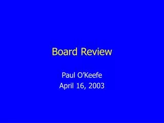
P3K FPDP Carrier Board Review Dean Palmer Building 318, Room 125 November 10, 2009 8:00 am – 12:00 pm
Presentation Outline • Introduction • Link Requirements • Link Components • Board Requirements • Board Design • FPGA Design • Schedule • Discussion
Introduction • Purpose • Provide a high speed data link system which connects distributed devices (RTC Subsystem) through a highly specialized communications protocol optimized for maximum data throughput to our active mirror electronics. • Data transfers occur without the CPU overhead and non-deterministic latencies associated with many layers of complex protocols • Must interface with the new mirror electronics as well as the old electronics • Must be able to maintain speed requirements over a length of 300’
Link Requirements • In order to keep the system loop delay small, the link speed must be fast and have low-latency. • The total time from first data out until the DM actuators are settled must be < 100 µsec (TBR).(< 50 µsec was desired but we know we can’t meet that.)We will try for < 70 µsec. • Xinetics first-in to all settled time is 37 µsec. (typ.) • This leaves about 30 µsec for the link transfer. • Required link data rate is about 226 MB/sec.(3388 chan. x 2 Bytes per chan.) / 30 µsec ~= 226 MB/sec
DM High-Speed Data Link Transmit End • Curtiss Wright FibreXtreme SL240 PCIe 2.5 Gb/s Data Link Card • Up to 247 MB/s per channel sustained data rate per channel • Low overhead ANSI/VITA 17.1-2003 Serial FPDP Protocol • Based on Fiber Channel. Uses similar ordered sets • Low latency (about 1us) • 4 independent channels
DM High-Speed Data Link Receive End • Curtiss Wright FibreXtreme SL240 CMC 2.5 Gb/s Data Link Card • IEEE P1386 Common Mezzanine Card form factor (same as PMC) • 32-bit parallel FPDP data bus @ 62.5 MHz • Custom Carrier Board • 6U VME form factor. FPGA based. • Four SOR-422U parallel output ports for connection to Xinetics Drivers. • P1 port for connection to LODM and TTM amplifiers.
P3K FPDP Carrier Board Requirements • The board must host the FPDP CMC card • Must provide physical area and mounting holes. • Must supply connectors for electrical interface. • Must supply power (3.3 VDC @ 1.4 A avg. 1.7 A peak) • The board must have an FPGA for processing data • Including power supplies and associated interfaces. • The board must have 4 outputs to Xinetics drive chassis. • The board must have a P1 interface for JPL chassis. • The board must provide Vref to JPL chassis. • The board must buffer Vmon from the JPL chassis • The board should have an A/D converter and mux. • The board should have 1 or 2 RS-232 ports (for future)
FPDP Carrier Board Block Diagram(Xinetics Interface) Configuration Curtiss Wright sFPDP CMC Module Xilinx Virtex-4 FPGA SOR422-U Output FPDP Transmit FPDP Receive SOR422-U Output SOR422-U Output RS-232 SOR422-U Output PROM, JTAG, Clock and Reset Analog Inputs 1.2V 2.5V 1.8V Core Voltage Regulators 5V to 3.3V Power Converter
FPDP Carrier Board Block Diagram(JPL Interface) Configuration Curtiss Wright sFPDP CMC Module Xilinx Virtex-4 FPGA FPDP Transmit FPDP Receive VME P1 Output (for LODM) RS-232 PROM, JTAG, Clock and Reset Analog Inputs 1.2V 2.5V 1.8V Core Voltage Regulators 5V to 3.3V Power Converter
FPDP CMC Board Interface • This board has three connectors • One connector, P3, is for configuration via fixed signals or a microprocessor interface • One connector, P4 is an FPDP transmitter. • One connector, P6 is an FPDP receiver.
RS-232 • Allows serial communications for future applications. • Borrowed design from Chris’s PZT driver board. • Benign design • single IC runs on 3.3V • built charge pumps for RS-232 rails
3.3 Volt Converter • Design borrowed from SIM Motor Board. • IC is a multi-chip module. • Input is 5 to 30 Volts. • Output current is 5 A continuous 7 A peak.
LT Spice Simulation of 3.3 V • 2 msec risetime on input power; 2 A load at power-up • Full Load (7 A) at 11 msec. Back to 2 A at 13 msec.
Core Power Regulators • Supplies 2.5V and 1.2V to the FPGA, Reset Circuit, and JTAG port. • Supplies 2.5V and 1.8V to the PROM. • Circuit design borrowed from Avnet Virtex-4 evaluation board. • Also used on SIM Motor Board. • Uses linear regulators.
SOR-422U Output Ports • Xinetics proprietary interface and protocol. • Uses LVDS Signaling. Using DS90LV047A driver IC.
SOR-422U Output Ports (cont.) Mini D Ribbon (MDR) connector Using Micro-strip traces (except on ready signal). This minimizes vias and stubs. There are actually five of these devices
SOR-422U Cables • We plan on clocking the SOR-422U ports at 62.5 MHz. This requires us to pay attention to the quality of the interconnect. • We plan on using a COTS cable made by 3M • Designed for LVDS signaling. • Contains 20 shielded 100 Ohm pairs + 6 grounds. • High-Density 50 position MDR connector. • Part number for 1m cable: 14150-EZBB-100-0LC • This cable requires an adapter and short ribbon cable at the Driver Chassis end to go from MDR to a standard 50-pin header.
SOR-422U Cables (cont.) Notice how the signal order reverses at opposite ends (except Link and ICMB).
Analog Inputs • Provide a test input for optional use if needed. • Could be used for test waveforms • Could be used for current monitor for JPL Drive • Plan on adding an analog mux for power supply monitoring.
Analog Inputs (cont.) • Analog ground plane pour on top layer. • +5VA and –5VA plane pours on Mid-Layer 3 and 4 • +2.5VA plane pour on Mid-Layer 2.
VME P1 Interface (for JPL board) • This interface is the same as used on the present DM receiver board except for the bus transceiver IC’s • Using the SN74VMEH22501A device made especially for driving VME backplanes. These devices use 3.3 volt signaling but are 5V tolerant. • The analog portion (Vref and Vmon) portions are virtually the same except for a few minor changes suggested by Chris Shelton. Digital Portionof Interface