Download
1 / 25
260 likes | 372 Views
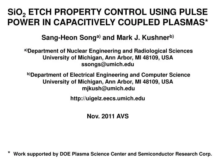
SiO 2 ETCH PROPERTY CONTROL USING PULSE POWER IN CAPACITIVELY COUPLED PLASMAS * Sang-Heon Song a) and Mark J. Kushner b) a) Department of Nuclear Engineering and Radiological Sciences University of Michigan, Ann Arbor, MI 48109, USA ssongs@umich.edu

E N D
SiO2 ETCH PROPERTY CONTROL USING PULSE POWER IN CAPACITIVELY COUPLED PLASMAS* Sang-Heon Songa) and Mark J. Kushnerb) a)Department of Nuclear Engineering and Radiological Sciences University of Michigan, Ann Arbor, MI 48109, USA ssongs@umich.edu b)Department of Electrical Engineering and Computer Science University of Michigan, Ann Arbor, MI 48109, USA mjkush@umich.edu http://uigelz.eecs.umich.edu Nov. 2011 AVS * Work supported by DOE Plasma Science Center and Semiconductor Research Corp.
University of Michigan Institute for Plasma Science & Engr. AGENDA • Motivation for controllingf(e) • Description of the model • Typical Ar/CF4/O2 pulsed plasma properties • Etch rate with variable blocking capacitor • Etch property with different PRF • Etch rate, profile, and selectivity • Concluding Remarks SHS_MJK_AVS
k CF3 + F + e e + CF4 University of Michigan Institute for Plasma Science & Engr. CONTROL OF ELECTRON KINETICS–f() • Controlling the generation of reactive species for technological devices benefits from customizing the electron energy (velocity) distribution function. SHS_MJK_AVS
University of Michigan Institute for Plasma Science & Engr. ETCH RATE vs. FLUX RATIOS • Large fluorine to ion flux ratio enhances etching yield of Si. • Large fluorocarbon to ion flux ratio reduces etching yield of Si. Etching Yield (Si/Ar+) Etching Yield (Si/Ar+) Flux Ratio (F/Ar+) Flux Ratio (CF2/Ar+) Ref: D. C. Gray, J. Butterbaugh, and H. H. Sawin, J. Vac. Sci. Technol. A 9, 779 (1991) SHS_MJK_AVS
p-Si p-Si University of Michigan Institute for Plasma Science & Engr. ETCH PROFILE vs. FLUX RATIOS • Large chlorine radical to ion flux ratio produces an undercut in etch profile. • Etch profile result in ECR Cl2 plasma after 200% over etch with different flux ratios • Flux Ratio (Cl / Ion) = 0.3 • Flux Ratio (Cl / Ion) = 0.8 Ref: K. Ono, M. Tuda, H. Ootera, and T. Oomori, Pure and Appl. Chem. Vol 66 No 6, 1327 (1994) SHS_MJK_AVS
University of Michigan Institute for Plasma Science & Engr. HYBRID PLASMA EQUIPMENT MODEL (HPEM) Te,Sb, Seb, k Fluid Kinetics Module Fluid equations (continuity, momentum, energy) Poisson’s equation Electron Monte Carlo Simulation E,Ni, ne • Fluid Kinetics Module: • Heavy particle and electron continuity, momentum, energy • Poisson’s equation • Electron Monte Carlo Simulation: • Includes secondary electron transport • Captures anomalous electron heating • Includes electron-electron collisions SHS_MJK_AVS
University of Michigan Institute for Plasma Science & Engr. MONTE CARLO FEATURE PROFILE MODEL (MCFPM) • The MCFPM resolves the surface topology on a 2D Cartesian mesh. • Each cell has a material identity. Gas phase species are represented by Monte Carlo pseuodoparticles. • Pseuodoparticles are launched with energies and angles sampled from the distributions obtained from the HPEM • Cells identities changed, removed, added for reactions, etching deposition. HPEM PCMCM Energy and angular distributions for ions and neutrals • Poisson’s equation solved for charging MCFPM Etch rates and profile SHS_MJK_AVS
University of Michigan Institute for Plasma Science & Engr. REACTOR GEOMETRY: 2 FREQUENCY CCP • 2D, cylindrically symmetric • Ar/CF4/O2 = 75/20/5, 40 mTorr, 200 sccm • Base conditions • Lower electrode: LF = 10 MHz, 500 W, CW • Upper electrode: HF = 40 MHz, 500 W, Pulsed SHS_MJK_AVS
PULSE POWER University of Michigan Institute for Plasma Science & Engr. • Use of pulse power provides a means for controlling f(). • Pulsing enables ionization to exceed electron losses during a portion of the ON period – ionization only needs to equal electron losses averaged over the pulse period. Pmax Power(t) Duty Cycle Pmin Time = 1/PRF • Pulse power for high frequency. • Duty-cycle = 25%, PRF = 50, 100, 200, 415, 625 kHz • Average Power = 500 W SHS_MJK_AVS
University of Michigan Institute for Plasma Science & Engr. VARIABLE BLOCKING CAPACITOR • Due to the different area of two electrodes, a “dc” bias is produced on the blocking capacitor connected to the substrate electrode. • The temporal behavior of “dc” bias is dependent on the magnitude of the capacitance due to RC delay time. • We investigated variable blocking capacitor of 10 nF, 1 mF, and 100 F • 100 F of blocking capacitor results in NO “dc” bias on the substrate. SHS_MJK_AVS
Typical Plasma Properties SHS_MJK_AVS
University of Michigan Institute for Plasma Science & Engr. MAX MIN PULSED CCP: Electron Density & Temperature • Electron Density (x 1011 cm-3) • Electron Temperature (eV) • Pulsing with a moderate PRF duty cycle produces nominal intra-cycles changes in [e] but does modulate Te. • 40 mTorr, Ar/CF4/O2=75/20/5 • PRF = 100 kHz, Duty-cycle = 25% • HF = 40 MHz, pulsed 500 W • LF = 10 MHz, 250 V ANIMATION SLIDE-GIF SHS_MJK_AVS
University of Michigan Institute for Plasma Science & Engr. MAX MIN PULSED CCP: ELECTRON SOURCES • by Bulk Electrons (x 1014 cm-3 s-1) • by Secondary Electrons • The electrons have two groups: bulk low energy electrons and beam-like secondary electrons. • The bulk electron source is negative due to electron attachment and dissociative recombination. • The electron source by beam electrons compensates the electron losses and sustains the plasma. ANIMATION SLIDE-GIF • 40 mTorr, Ar/CF4/O2=75/20/5 • LF 250 V, HF 500 W SHS_MJK_AVS
University of Michigan Institute for Plasma Science & Engr. PULSED CCP: E-SOURCES and f(e) • Rate coefficient of e-sources is modulated between electron source (electron impact ionization) and loss (attachment and recombination) during pulsed cycle. ANIMATION SLIDE-GIF • 40 mTorr, Ar/CF4/O2=75/20/5 • PRF = 100 kHz, Duty-cycle = 25% • LF = 10 MHz, 250 V • HF = 40 MHz, pulsed 500 W SHS_MJK_AVS
Etch Properties:Variable Blocking Capacitor SHS_MJK_AVS
University of Michigan Institute for Plasma Science & Engr. PULSED CCP: PLASMA POTENTIAL & dc BIAS • A small blocking capacitor allows the “dc” bias to follow the change during the pulse period. • Maximum ion energy gain = Plasma Potential – “dc” Bias • 1 mF • 10 nF • PRF = 100 kHz, Duty-cycle = 25% • LF = 10 MHz, 250 V • HF = 40 MHz, pulsed 500 W
University of Michigan Institute for Plasma Science & Engr. ETCH PROFILE IN SiO2 & IEAD: 1 mF • With constant voltage, bias amplitude is constant but blocking capacitor determines “dc” bias. • Cycle Average IEAD • Etch Profile (600 sec) Energy (eV) Height (mm) Width (mm) Angle (degree) ANIMATION SLIDE-GIF SHS_MJK_AVS • Pulsed HF 40 MHz 500 W • LF 10 MHz 250 V, Blocking Cap. = 1 mF
University of Michigan Institute for Plasma Science & Engr. ETCH PROFILE IN SiO2 & IEAD: 10 nF • With smaller blocking capacitor, “dc” bias begins to follow the rf power and so produces a different IEAD. • Cycle Average IEAD • Etch Profile (600 sec) Energy (eV) Height (mm) Width (mm) Angle (degree) ANIMATION SLIDE-GIF SHS_MJK_AVS • Pulsed HF 40 MHz 500 W • LF 10 MHz 250 V, Blocking Cap. = 1 nF
University of Michigan Institute for Plasma Science & Engr. ETCH PROFILE IN SiO2 & IEAD: NO dc BIAS • In absence of dc bias and for constant voltage, pulse power and is effect on f() in large part determine etch properties. • Cycle Average IEAD • Etch Profile (600 sec) Energy (eV) Height (mm) Width (mm) Angle (degree) ANIMATION SLIDE-GIF SHS_MJK_AVS • Pulsed HF 40 MHz 500 W • LF 10 MHz 250 V, Blocking Cap. = 100 F
University of Michigan Institute for Plasma Science & Engr. POWER NORMALIZED ER: Blocking Capacitor • Power normalized etch rate is dependent not only on the pulse repetition frequency (PRF), but also the value of the blocking capacitor on the substrate at lower PRF. • F to Poly Flux ratio C B A CW 250 100 50 kHz C B A • Pulsed HF 40 MHz 500 W • LF 10 MHz 250 V SHS_MJK_AVS
University of Michigan Institute for Plasma Science & Engr. E-SOURCES and FLUX RATIO: PRF • Electron source rate coefficient is modulated with f(e) by pulse power. • Modulation is enhanced with smaller PRF. • F to Poly Flux ratio • Pulsed HF 40 MHz 500 W • LF 10 MHz 250 V • Blocking Cap. = 1 mF SHS_MJK_AVS
University of Michigan Institute for Plasma Science & Engr. ETCH RATE: POWER NORMALIZED • Power normalized etch rate is large at 250 kHz with ion distribution extending to higher energies. • Cycle Average IEAD • Normalized Etch Rate Energy (eV) CW 250 100 50 kHz Angle (degree) • Pulsed HF 40 MHz 500 W • LF 10 MHz 250 V • Without DC Bias on LF electrode SHS_MJK_AVS
University of Michigan Institute for Plasma Science & Engr. ETCH PROFILE: CRITICAL DIMENSION • CD is compared at the middle and bottom of feature. • CW excitation produces bowing and an undercut profile. • Pulse plasma helps to prevent the bowing and under-cutting. • Smaller PRF has a tapered profile. • EPD + Over Etch 50% A (1/A) 1 (2/A) CW 250 100 50 kHz 2 • Pulsed HF 40 MHz 500 W • LF 10 MHz 250 V • Blocking Cap. = 1 mF SHS_MJK_AVS
University of Michigan Institute for Plasma Science & Engr. ETCH SELECTIVITY: Between SiO2 and Si • Silicon damage depthis compared in 2-D etch profile. • Pulsed operation helps to prevent the silicon damage. • Lower damage appears to be correlated with smaller F flux ratio at 250 kHz. • EPD + Over Etch 50% CW 250 100 50 kHz • Pulsed HF 40 MHz 500 W • LF 10 MHz 250 V • Blocking Cap. = 1 mF SHS_MJK_AVS
University of Michigan Institute for Plasma Science & Engr. CONCLUDING REMARKS • Extension of tail of f(e) beyond that obtained with CW excitation produces a different mix of fluxes to substrate. • Etch rate can be controlled by pulsed operation with different pulse repetition frequencies. • Blocking capacitor is another variable to control ion energy distributions and etch rates. Smaller capacitance allows “dc” bias to follow the plasma potential in pulse period more rapidly. • Etch rate is enhanced by pulsed power operation in CCP. • Etch profile is improved with pulsed operation preventing undercut. • Etch selectivity of SiO2 to Si is also improved with PRF of 250 kHz with a smaller fluorine flux ratio. SHS_MJK_AVS