Download
1 / 17
470 likes | 2.7k Views
Silicon Etching Using Inductively Coupled Plasma Etching. Drew Sellers ELEC 6750 Spring 2004. Questions. What are the benefits of using inductively coupled plasma etching systems? What are the two different types of inductively coupled plasma coil configurations?. Outline.

E N D
Silicon Etching Using Inductively Coupled Plasma Etching Drew Sellers ELEC 6750 Spring 2004
Questions • What are the benefits of using inductively coupled plasma etching systems? • What are the two different types of inductively coupled plasma coil configurations?
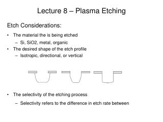
Outline • Definitions of terms • History of silicon plasma etching • General ICP etching system configuration • Problems associated with ICP etching systems • Effects of coil operation on plasma concentration
Introduction • Microelectronic fabrication often requires the etching of silicon substrates to form intricate structures for proper device function. In order to make this possible, fabricators have employed the use of inductively coupled plasma etching systems. The following presentation offers a brief description of a typical ICP system, along with its benefits in microelectronic fabrication.
Definitions of Terms • ICP – inductively coupled plasma • RIE – reactive ion etcher • DRIE – deep reactive ion etcher • Anisotropic – etched surface is attacked faster in the horizontal plane than the lateral plane
History of Silicon Plasma Etching • Barrel reactors • Inductively coupled barrel reactor • Capacitively coupled barrel reactor • Parallel plate reactor • Reactive ion etcher
Barrel Reactors • Inductively coupled barrel reactor • AC voltage source connected across the ends of a coiled winding • Capacitively coupled barrel reactor • AC voltage source connected between inner and outer walls http://www.triontech.com/techPapers/plasmaBasics.html
Parallel Plate Reactor • Substrate platform powered by an AC voltage source • Chamber wall connected to ground to form a capacitive structure http://www.triontech.com/techPapers/plasmaBasics.html
Reactive Ion Etcher • AC voltage source connected entirely beneath wafer surface • Ions in plasma are accelerated toward the substrate surface • Enabled fabricators to produce the first anisotropic etching systems http://www.triontech.com/techPapers/plasmaBasics.html
The ICP Etching System • Employs aspects of all three basic etching systems • Requires the use of two RF power sources • RIE – forms the plasma potential at the surface of the substrate • ICP – enhances the amount of reactive species in the chamber "Silicon Micromachining Using a High-Density Plasma Source," J. Appl. Phys., Vol. 34, 2001, pp. 2769-2774
ICP Coil Configuration • Two types of coils • Spiral – also known as “stove-top” coil • Helical – coiled in the shape of a helix http://images.google.com/images?q=coil&hl=en&lr=UTF-8Qoe=UTF-8&start=20&sa=N
Spiral Coiled ICP Sources • Require the use of an additional capacitive circuit element in order to tune the inductor for electrical resonance at the input RF
Helical Coiled ICP Sources • Do not require the use of an additional capacitive circuit to achieve RF resonance • Uses a grounded RF shield and the coil to achieve RF resonance • Heating profile can be adjusted easily by moving RF tap along the coil
Problems with ICP Etching Systems • Wafer clamping structures within the chamber can cause diffusion losses "Silicon Micromachining Using a High-Density Plasma Source," J. Appl. Phys., Vol. 80, No. 3, 1 August 1996, pp. 1337-1344
Problems with ICP Etching Systems • Increased areas around chamber doors allow plasma to form at higher densities in these areas "Silicon Micromachining Using a High-Density Plasma Source," J. Appl. Phys., Vol. 80, No. 3, 1 August 1996, pp. 1337-1344
Conclusion • Through the aid of plasma etching, engineers are able to produce smaller, more precise structures • Inductively coupled plasma etchers allow fabricators to control more aspects of the etching process, and therefore more control in the etch results
Answers to Questions • What are the benefits of using inductively coupled plasma etching systems? • Faster etch rates, cleaner and more selective etches, and much lower operating voltages at the sample surface • What are the two different types of inductively coupled plasma coil configurations? • Spiral and helical