Download
1 / 9
90 likes | 168 Views
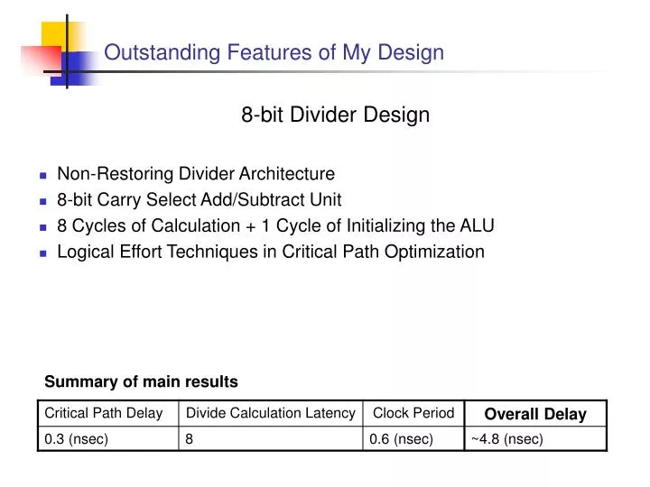
Outstanding Features of My Design. 8-bit Divider Design Non-Restoring Divider Architecture 8-bit Carry Select Add/Subtract Unit 8 Cycles of Calculation + 1 Cycle of Initializing the ALU Logical Effort Techniques in Critical Path Optimization. Summary of main results.

E N D
Outstanding Features of My Design 8-bit Divider Design • Non-Restoring Divider Architecture • 8-bit Carry Select Add/Subtract Unit • 8 Cycles of Calculation + 1 Cycle of Initializing the ALU • Logical Effort Techniques in Critical Path Optimization Summary of main results
Divider Architecture Introduction: The goal of this project is to design an 8-bit binary divider with minimum overall delay it takes to perform a divide operation. The delay is comprised of the number of clock cycles needed to perform a computation multiplied by the clock period, Delay = Ncycles·TClk. To find optimal compromise between Ncycles and TClk in such a way as to minimize the overall delay of the divide operation. Start: Place Dividend in Remainder 1. Subtract the Divisor register from 7-14 bit of the Remainder register and place the result to the Remainder register. 2a. Subtract the Divisor register from the 7-14 bit of the Remainder register and place the result to the Remainder register. 2b. Add the Divisor register from the 7-14 bit of the Remainder register and place the result to the Remainder register. Remainder >=0 Test Remainder Remainder < 0 Design Methodology: 1.Schematic: Normally, there are two dividing algorithm (Resorting and Non-Resorting) that we can apply to our design. As we want to minimize the overall delay that it takes to perform a division, we choose the Non-Resorting algorithm, which can give us fewer cycles and operation of calculation. 3a. Shift the Quotient register setting the rightmost bit to 1 and 0-6 bit of Remainder to the left setting the rightmost bit to 0. 3b. Shift the Quotient register setting the rightmost bit to 0 and 0-6 bit of Remainder to the left setting the rightmost bit to 0. nth repetition? nth repetition? No: < n repetitions No: < n repetitions Divisor Yes: n repetitions (n = 8 here) Yes: n repetitions (n = 8 here) Quotient Add/Subtract Shift Left Adder Shift Left Control DONE Remainder
8 Bit Shift Register w/ Reset (Quotient) • 8 Bit Shift Register w/ Reset (Dividend bit 0-7) Divider Schematic • 8 Bit Register (Divisor) • 1 Bit Register • 8 Bit Register w/ Reset (Remainder bit 8-15) 2.Connection Design: As a given parameter that divisor is positive, we can reduce one cycle by connecting the 7-14bit of the remainder to the input of our 8bit adder. And, it turns out that we need 8 cycles to finish our 8bit/8bit calculation.
Carry Select Architecture Detailed Schematics We are using a Mirror Adder to form a 4-bit-adder. Exploiting the inverting property, we arrange the adder cells in the following way. To get a faster result of addition, we choose carry select to connect two 4-bit-adders to form an 8-bit-adder. 3.Adder Design: For a Non-Restarting schematic, we need both add and subtract operation. To build an 8bit Add/Subtract Unit, we use three 4bit adder. The first 4bit adder which inputs are connected by XOR(make is changeable from add/sub) generate SUM0 to SUM3 and COUT3. The 2nd 4bit adder used to generate SUMs that COUT3=1. The 3rd 4bit adder used to generate SUMs that COUT3=0. Finally, we select our output by using a MUX. 8 Bit Shift Register w/ Reset 4 Bit Ripple Adder Transmission Gate XOR Multiplexor 8 Bit Carry Select Adder
Functionality Verification Quotient Remainder Quotient Valid Result Remainder Valid Result
Critical Path Worst Case Input(Consider 4 LSBs): Remainder: 0000 0101 Divisor: 0000 0101 We have subtraction in the first cycle: 0000 0101 0000 0101 -) 0000 0101 1111 1010 +) 1 0000 0000 25 CUNIT MUX ADDER XOR MUX 4. Critical Path: Critical path exist between registers. We calculate the critical path by using logical effort. First, we assume the logical effort of our OXR is 3 and MUX is 3 for “reset” and 2 for input. By taking out the critical path and separate it into 9 stages(such as Full-Adder, OXR, INV, MUX) we calculate GHF and find that h=7.63. Using the load of 25unit load, we find the each size of the stages from the back.
Critical Path Sizing • Path Logical Effort: • G = G1 x G2 x … x Gn = 1 x 1 x 3 x 8 x 6 x 6 x 6 x 3 x 2 • Branching Effort: • B = B1 x B2 x … x Bn = 9 x 2 x 2 x 2 x 2 x 5 • Path Electrical Effort: • F = Cout/Cin = 25/1 = 25 • Path Effort: • H = G x B x F = 559872000 • Total Stages: 10 • Effective Fanout for each stage: h = H^(1/10) = 7.4956 7.4956 6.24275 15.5978 7.307 4.564 2.851 0.71235 0.8899 6.6705
Other Design Approach & Schematics 4 Adders in a Divider 2 Adders in a Divider 5. Extra Designs(Design Improvement): The above figures show 2 different improved design approach. There are 2 and 4 eight-bit-adders in the devices. The purpose of doing this is that we can eliminate the register delay time between each addition by providing a longer clock period. This method needs much longer clock period because of the loading of stacks of adders, but it can reduce the numbers of clock cycles and the treg. In the beginning of the design process, we used only one adder in the divider. However, we found out that we could do two or more additions in a longer clock cycle. Thus, there was only one adder in our first generation and two adders in the second generation, and finally, to the last design of 4 adders in one divider. (due to the limitation of 4 adder modules in the design)
Conclusion In this project, we’ve experienced the optimization process of the adder and the divider. We believe that every design always has a better solution. We first came up with the one adder in a divider, then 2 adders, and finally 4 adders. However, the critical path of the 4-adder-divider can not be easily analyzed. Thus, we back off to our original design. The 4-adder-divider indeed is faster, but it’s much more complicated than the 1-adder-divider that we think it’s not worth to tradeoff the simplicity to gain that little speed. If we have more time with the project, there’s always a better and faster design for the divider.