Download
1 / 17
170 likes | 178 Views
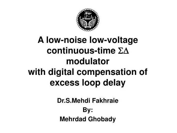
A low-noise low-voltage continuous-time SD modulator with digital compensation of excess loop delay. Dr.S.Mehdi Fakhraie By: Mehrdad Ghobady. Outline. Introduction Quantization Error and Oversampling Decimation Process Delta Modulation Sigma-Delta Modulation

E N D
A low-noise low-voltage continuous-time SD modulator with digital compensation of excess loop delay Dr.S.Mehdi Fakhraie By: Mehrdad Ghobady
Outline • Introduction • Quantization Error and Oversampling • Decimation Process • Delta Modulation • Sigma-Delta Modulation • Sigma-Delta Modulator Architecture • Performance Summary • References
Introduction • The performance of digital signal processing and communication systems is generally limited by the precision of the digital input signal which is achieved at the interface between analog and digital information. • Sigma - delta modulation based analog -to- digital (A/D) conversion technology is a cost effective alternative for high resolution (greater than 12 bits)converters which can be ultimately integrated on digital signal processor ICs.
Quantization Error and Oversampling • Nyquist rate A/D converter • Oversampling A/D converter Fig.4:Frequency Response of Analog Anti-Aliasing Filters[2]
Decimation Process Fig.5:Simple Example of Decimation Process[2]
Delta Modulation Fig.6:Delta Modulation and Demodulation[2]
Sigma-Delta Modulation Fig.7:Derivation of Sigma-Delta Kodulation from Delta Modulation[2]
Sigma-Delta Modulation Fig.8:Block Diagram of Sigma-Delta Modulation[2]
S-Domain Analysis of Sigma Delta Modulator Fig.9:S-Domain Analysis[2]
Block Diagram of First-Order Sigma-Delta A/D Converter Fig.10:First-Order Sigma-Delta Converter[2]
Sigma-Delta Modulator Architecture Fig.11:Sigma-Delta Modulator Architecture[1]
The noise transfer function (NTF) has a pair of complex zeros judiciously chosen to maximize the SQNR in the bandwidth of interest ,and created by the local feedback. • The poles of the modulator (coefficients ai) represent 3rt order approximation. • Feedforward paths (coefficients bi) are used to reduce the dynamics at the output of the first integrator ,thus improving the overall linearity of the modulator.
Performance Summary Table.1:Performance Summary of Sigma-Delta Modulator[1]
References • [1] Paul Fontaine, Ahmed N.Mohieldin , Abdellatif Bellaouar ,” A Low-Noise Low-Voltage CT Delta-Sigma ModulatorWithDigital Compensation of Excess Loop Delay, “ JSSCC 2005. • [2] Sangil Park , “ Principles of Sigma-Delta Modulation for Analog-to-Digital Convertors” , MOTOROLA. • [3] David Jarman , “A Brief Introduction to Sigma-Delta Conversion” ,1995.