Download
1 / 36
360 likes | 457 Views
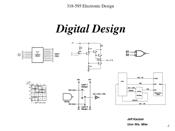
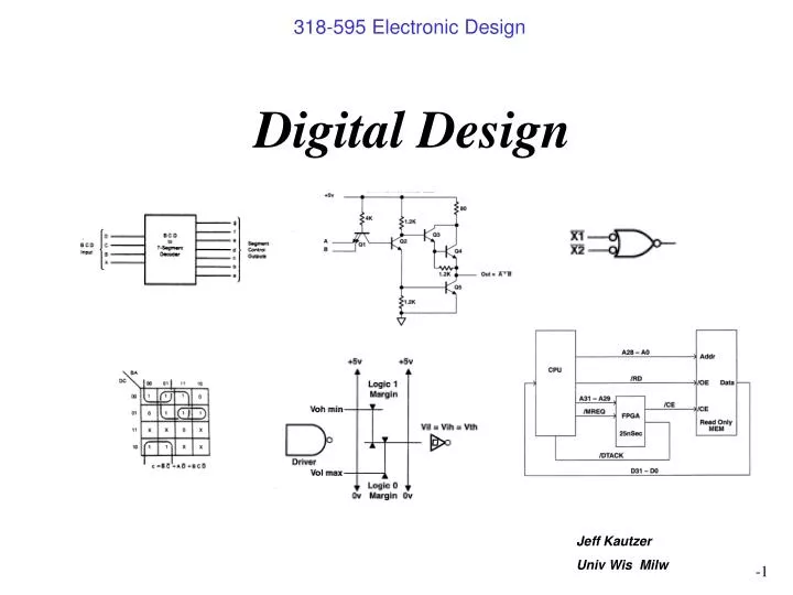
Digital Design. Jeff Kautzer Univ Wis Milw. Review: Digital Information. Information is represented numerically using a binary number system An n bit number has digit weightings 2 (n-1) 2 (n-2) 2 (n-3) ……. 2 1 2 0 Example: 11010b = 2 4 + 2 3 + 2 1 = 26

E N D
Digital Design Jeff Kautzer Univ Wis Milw
Review: Digital Information • Information is represented numerically using a binary number system • An n bit number has digit weightings 2(n-1) 2(n-2) 2(n-3) ……. 21 20 • Example: 11010b = 24 + 23 + 21 = 26 • 4 bit binary “nibbles” are abbreviated using hexidecimal • 1001b = 9h, 1010b = Ah, 1011b = Bh, ….. 1111b = Fh • Logic 1: Represented by a high voltage level and/or forward current • Logic 0: Represented by a low voltage level and/or reverse current • Binary numbers are conveyed individually in time between two or more digital devices. • Devices have electrical limitations in drive, speed, distance, & fanout • Devices may share the same wires/nodes using time based multiplexing
Review: Basic 2 Input Logic Operators Gates and their Demorgan Equivalents Note: A Bubble implies logic inversion
Review: Truth Tables, Karnaugh Maps N = 4 Grey Code
Example: Binary-7Segment Display Decoder 2 Types of Display Configurations Vcc Common Cathode LEDS Active High Common Anode LEDS Active Low Gnd
7 Segment Display 7- segment used to form digits 0-9
Commercial TTL BCD-to-7-segment decoder/driver driving a common-anode 7-segment LED display; 7447 segment patterns for all possible input codes.
Truth Table for Active High (Common Cathode Display Drive) Hex Digits A-F not defined by this decoder. All Segments OFF
Truth Tables and MIN Terms • Each line in the Truth Table is Represented by a “MIN” Term • Each MIN Term is a Full Expression containing each input variable • For Output “a” the following MIN Terms would be Logically “OR”d DCBA DC B A DC B A D C B A D C B A D C B A D CBA Note: X = NOT X D CB A Output a = DCBA + DC B A + DC B A + D C B A + D C B A + D C B A + D CBA + D CB A
Truth Table Reduction • Two MIN Terms can be combined if the same output is obtained but the input variable values differ in only 1 bit position. • The variable for which the value differs with no effect on output is eliminated from the resulting expression. DC B D C B CBA D CB
Combining Adjacent Cells (Min Terms) Reduces Logic Implementation Output a = DCBA + DC B A + DC B A + D C B A + D C B A + D C B A + D CBA + D CB A • 8 Min Terms …. 1 Eight Input OR Gate + 8 Four Input AND Gates + 4 Inverters • Total of 9 Four Input Gates + 4 Inverters Karnaugh Map Combinations AC B D A C D Output a = B D + C D + AC + A C D • 8 Min Terms …. 5 Four Input Gates + 3 Inverters • Total of 8 Gates, Smaller Gates with Fewer Inputs C D
Liquid-Crystal Displays Liquid-crystal display: (a) basic arrangement; (b) applying a switching voltage between the segment and the backplane turns ON the segment. Zero voltage turns the segment OFF.
Commerical Logic devices for driving an LCD segments and full 7-segment displays
Common XOR Reduction Patterns (Alternating Columns, Quads, and Pairs, Checkerboards)
Digital IC Technologies/Families • Bipolar: Utilizes BJT’s exclusively as switching elements. Originated by Fairchild/TI, families have included STD, L, H, LS, S, ALS, AS and F • pp74xxx###P Standard Part Numbering Scheme Package Suffix (Plastic, Ceramic, DIP, SOJ, etc) Generic Device Function Number (Ex. 244 Octal Driver) Family Designation (Ex. ALS, AS, F, etc) 7 =Commercial (0-70C), 5 =Military (-55 to 125C or more) Mfg Prefix (Ex. SN = Texas Inst, DM = Fairchild, etc) Example Function/Family Package Options For Family Examples see: http://focus.ti.com/logic/docs/logicportal.tsp?templateId=5985&DCMP=TIHomeTracking&HQS=Other+OT+home_p_logic
Active Bipolar Logic Families ALS Advanced Low-Power Schottky Logic AS Advanced Schottky Logic F Fast Logic LS Low-Power Schottky Logic S Schottky Logic TTL Transistor-Transistor Logic (STD)
C B E • Review: Schottky Diode • PN Junction Si Diode Similar to std diode • Low Forward Voltage Drop (~0.3V) • Schottky Transistor • Schottky Diode from Collector to Base of NPN switching transistor • Vbc < Vf of Schottky Diode (~0.3V) • Vce-sat (schottky) > Vce-sat (std BJT) • Base-Collector Clamp prevents hard saturation • Switches Faster as a result
Digital IC Technologies/Families • CMOS: Utilizes C-MOSFETs exclusively as switching elements. Originated with 4000 series family (still produced) followed with C, HC, HCT, AC, ACT, FCT, LV, LVC and many others (see list) • Devices follow Bipolar part numbering scheme (except for 4000 series) • Characterized by • Very low input current (leakage current) • Symmetric Output drive currents • Device size/process scales. Industry has moved from 5um channels to less than 75nm channels in < 30 yrs Example: HC, HCT Families Function/Family Package Options
ACTIVE CMOS Logic Families AC Advanced CMOS Logic (1.5 to 5.5V typ) ACT Advanced CMOS Logic AHC Advanced High-Speed CMOS (2.0 to 5.5V typ) AHCT Advanced High-Speed CMOS ALVC Advanced Low-Voltage CMOS Technology (2.3 to 3.6V typ) AUC Advanced Ultra-Low-Voltage CMOS Logic (0.8 to 2.7V typ) AUP Advanced Ultra-Low-Power CMOS Logic (0.8 to 2.7V typ) AVC Advanced Very-Low-Voltage CMOS Logic (0.8 to 2.7V typ) CB3Q Low-Voltage, High-Bandwidth Bus Switch Technology CB3T Low-Voltage, Translator Bus Switch Technology CBT Crossbar Technology CBT-C CBT with Undershoot Protection CBTLV Low-Voltage Crossbar Technology CD4000 CMOS Logic (4000 Series, 3 to 18V typ) FCT Fast CMOS Technology GTLP Gunning Transceiver Logic Plus HC High-Speed CMOS Logic (2.0 to 6.0V typ) HCT High-Speed CMOS Logic LV-A Low-Voltage CMOS Technology (2.0 to 5.5V typ) LV-AT Low-Voltage CMOS Technology LVC Low-Voltage CMOS Technology (1.6 to 3.6V typ) PCA Inter Integrated Circuit PCF Inter Integrated Circuit SSTV Stub Series Terminated Low-Voltage Logic TVC Translation Voltage Clamp VME VME Bus Products
Other Digital IC Semiconductor Technologies • BiCMOS: Combination CMOS/BJT. Can be implemented using Si but SiGe becoming popular for mixed signal applications. Families include: HSTL, BCT, FB, ABT, ALB, LVT and others (see list) • ECL/LVDS: Emitter Coupled Logic / Low Voltage Differential Signaling. Si BJT or CMOS devices that utilize differential signaling with extremely low voltage swings. Typically seen on the output from A/D conversion circuits. Switching speeds > 60Mhz. • GaAs: FET based devices with extremely fast switching and delay characteristics. Ft > 10Ghz easily achievable. Costs > 20X that of fast CMOS
Active BiCMOS Logic Families ABT Advanced BiCMOS Technology ABTE Advanced BiCMOS Technology / Enhanced Transceiver Logic ALB Advanced Low-Voltage BiCMOS (3.0 to 3.6V typ) ALVT Advanced Low-Voltage CMOS Technology (2.3 to 3.6V typ) BCT BiCMOS Technology FB Backplane Transceiver Logic GTL Gunning Transceiver Logic HSTL High-Speed Transceiver Logic JTAG JTAG Boundary Scan Support LVT Low-Voltage BiCMOS Technology (2.7V to 3.6V typ) SSTL Stub Series Terminated Logic
Other Aspects of Technology:Component Life Cycle Phases • = Mean (Max) Sales of Unit Components per Unit Time s = One Standard Deviation in Sales/Time
Life Cycle of a Component • Special Histogram of Production as Measure by Component Sales/Time (# shipped/time) • Concept Assumes Component Sales follow monotonically increasing to peak, then monotonically decreasing to obsolesence • Life Cycle is Measured Relative to Peak of Sales • +/- 1s from Peak = Mature Product • -1s to –2s from Peak = Growth Product • -2s to –3s from Peak = Introductory Product • +1s to +2s from Peak = Declining Product • +2s to +3s from Peak = Phase Out Product • +3s and higher from Peak = Obsolete Product
Logic Signal Electrical Characteristics • Finite Transition Time Zone • Driver must switch voltage thru this zone within specified time or risk causing linear operation of receiver ! • Typically < 1uS but varies with logic family technology
Logic Device Drive Parameters Note: Sourced currents are always listed as a negative number by convention on data sheets
Interpreting the Data Sheet Vih, Vil Ioh, Iol Voh @ Ioh (note max Ioh) Vol @ Iol (note max Iol) Iih, Iil
Device Output Structure Type 1: Totem Pole Current Limiting Resistor (reduced in modern devices) Top Voh/Ioh Source Driver (Switch to Vcc) Bottom Vol/Iol Sink Driver (Switch to Gnd) Cross-over of Q4:Q5 – ON/OFF may result in high current spike from Vcc to Gnd Octal and larger devices rated for “Gnd Bounce” Volp. Measure of Static output disturbance when all other outputs switch simultaneously.
Device Output Structure Type 2: Open Collector/Drain • Current Limiting Resistor Removed • Top Voh/Ioh Source Driver Removed • Bottom Vol/Iol Sink Driver • Sink Trans Q5 acts as a switch to Gnd • No inherent Logic 1 voltage drive • Interface in 2 ways; • Pullup resistor to Vcc to establish logic 1 voltage level • Switch current through load device (Ex. Relay Coil, LED, Lamp, Solenoid, etc) Note OC/OD Datasheets: May list Vce-sat for Vol, Ic max for Iol max, Vce max (off). Will NOT list Voh, Ioh values ! OC/OD Outputs will have very slow Logic 0 to 1 transition times !
OC/OD outputs may be tied together, Wire-OR Determining Pullup Resistor Limits • Maximum R - Limited by Logic 1 condition: R must supply Vih @ Iih to receiver plus supply any leakage current to the driver OFF transistors. Finite Current of Io flows thru R dropping voltage. Usually use R < 100KW • Minimum R - Limited by Logic 0 condition: Driver ON may cause Vol as low as 0V, Driver must sync Io from Vcc thru pullup resistor plus Iil source current from receiver. Total load current cannot exceed Driver Iol current capacity. Usually use R> 1KW
Device Output Structure Type 3: Tristate-able Current Limiting Resistor (reduced in modern devices) Top Voh/Ioh Source Driver (Switch to Vcc) Bottom Vol/Iol Sink Driver (Switch to Gnd) Q7/Q8 used to stop base current to Q3/Q4 darlington Turn off Source Driver Q2 used for same purpose but controls Sink Driver E turns OFF Q4 and Q5 simultaneously
Interpreting the Data Sheet Vcc Supply Voltage Range Normal Input Specs apply to Enable Input (G) Off State Output Leakage Currents Logic Level Dependent Icc Max Supply Current Note: Occurs when outputs in Hi Z
Multiplexing Drivers for Bus Operation • Active Driver must provide Iih/Iil currents to ALL receivers plus all the OFF state leakage currents of the other inactive Drivers • Must NOT have 2 or more Drivers Active simultaneously. Time Division multiplexing (timing) analysis critical to long term reliabililty of devices
Standard vs Schmitt Trigger Input Functions • Single Input Threshold Vth, Eliminates Undefined Transition Zone • Input should also have minimum “hysteresis” to provide noise immunity • As Vin increases thru Vth, Vth decreases by DV (Vhyst) • As Vin decreases thru Vth, Vth increases by DV (Vhyst) • Vth is typically 1.0 – 2.0 V, Vhyst should be > 200mV • Schmitt Trigger should always follow OC/OD outputs or other slow rise or fall time signals (Ex. Optocoupler Outputs, RC Reset Circuits, etc )
Basic Combinatorial Timing Parameters • TpHL(TpLH): Propagation Delay from High to Low (Low to High) Logic Level Usually measured between the 10% and 90% total voltage transition points. • Tpd or Tp: Propagation Delay usually stated as worst case of TpHL and TpLH. • Tott or Tout: Output Transition Time. For many families (HC, HCT, etc), gate delays are stated with separate specifications for logical output value generation (Tpd) plus physical output voltage transition (Tott). Need to sum these for total prop delay !! • TpzH(TpzL): Propagation Delay from High Impedance to High (Low) Logic Level • TpHz(TpLz): Propagation Delay from High (Low) Logic Level to High Impedance