Download
1 / 20
200 likes | 336 Views
First CCE and TCT measurements on irradiated diodes of the CMS-HPK-Campaign 24.05.2011. Robert Eber A. Dierlamm , Th.Müller , W. de Boer, P. Steck , Th. Pöhlsen (HH), Ch. Scharf (HH). Outline. Setups and Groups Preparation for TCT and CCE measurements Stability measurements

E N D
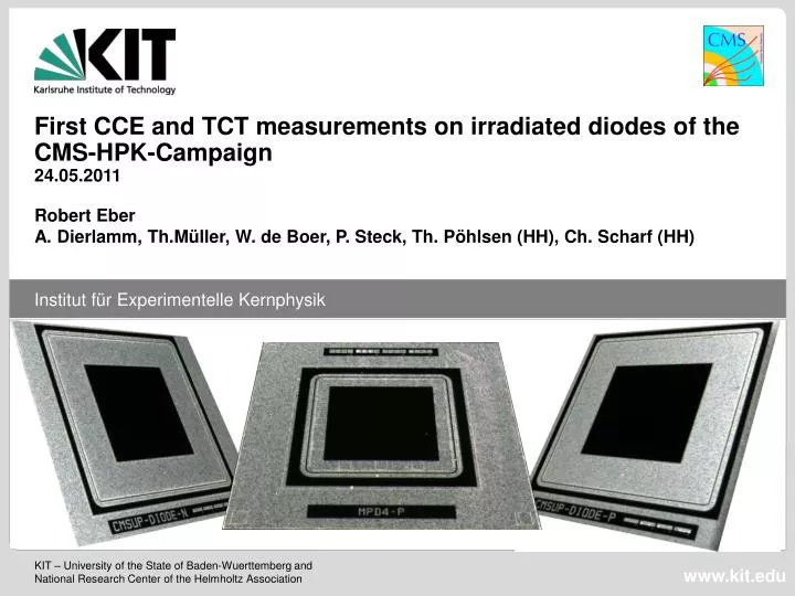
First CCE and TCT measurements on irradiated diodes of the CMS-HPK-Campaign 24.05.2011 Robert Eber A. Dierlamm, Th.Müller, W. de Boer, P. Steck, Th. Pöhlsen (HH), Ch. Scharf (HH)
Outline • Setups and Groups • Preparationfor TCT and CCE measurements • Stabilitymeasurements • Backsidemeasurementswith 880nm • Comparisonof FZ / MCz material • Charge Collectionof non-irradiateddiodes • CCE ofirradiateddiodes • TCT ofirradiateddiodes • Trappingtimes • Conclusionand Outlook
Setups for CCE and TCT measurements • Institutes involved in diodemeasurements • CERN, Hamburg, Louvain, Karlsruhe
Specificationsof CCE / TCT measurements • CCE measurements • Measurement ofchargecollection, simulationof a MIP • Integrated signalimportant • TCT measurements • Time resolvedcurves • Observation of 1 chargecarrierthroughthediode • Neededfortrappingtimesandelectricfield • Lasers: • >1000nm for CCE • Redfor TCT (~680nm) • 880nm forbackside TCT • Laser intensity < 100 MIPs • Repetition rate 200Hz • Min. 5GS/s Oscilloscope • Averagingofwaveforms > 500 • Measurement steps: • 0V-1000V in 10V steps • Nobreakdown • Non-irradiateddiodes • 20°C, 0°C, -20°C • Irradiateddiodes • 0°C, (-10°C), -20°C, (-30°C) • Severalannealingsteps
Backsidemeasurements • Backside TCT measurementsnot possible on thindiodesbecauseofdeepdiffusion • Signal generationpossible in • 320µm thick FZ diodes • 200µm MCzdiodes • Due torelativelydeepbacksideimplantationandbacksideproperties on FZ diodes – generationofchargecarriers not possiblewithred Laser (680nm) on FZ • IR Laser light shot an FZ backsidegeneratesonly ~20% offrontsidesignal MCz FZ
Backsidemeasurements • Red Laser workswellforMCzdiodes • Not a deepimplantation on thebackside – different processing • Back/front chargecollection ~ 80% • Forcomparison, FZ material with a physicalthicknessof 200µm isorderedand will arrive in autumnthisyear
Backsidemeasurements Penetration depth [µm] • Use 880nm Laser forillumination on thebacksidefor FZ material • Signal looksalmostlike a redone • Possibilitytolookatonechargecarrier in FZ 320µm material • Atlowvoltages • Broadsignalcomingfromdiffusion out ofthedeepdiffusionregion • Athighervoltages • Long tailsatthe end of signal • First smallpeak in signal due toelectrons (n-type diode) • Usefulforanalysis? Wavelength [nm]
CCE measurementofunirradiateddiodes • Signal generationwithinfrared Laser (1055nm) • Becauseofindirectbandgap in silicon, fewerchargecarriersareproduced • Calibratesignalfor different temperatures • Red Laser alwaysgeneratesthe same amountofchargecarrierswhenshot on frontside(irradiateddiodeexample) 320µm, n-type diode
CCE measurementofunirradiateddiodes • Signal generationwithinfrared Laser (1055nm) • CCE normalizedtothe 320µm thickdiodeof same type • Slightincrease in CCE(V) seenfor 200µm and 120µm thickdiodes • Gainmoreacitvethickness due todeepdiffusionat high voltages • Charge collectionratio in expectedrange • 63% for 200µm, (67% for 215µm) • 38% for 120µm, (45% for 145µm)
Charge collection on different wafers • Takingintoaccount • Attenuationlengthoflaser • Measuredthicknessfrom CV • Deviationsof max. 5% frommeanvalue [1] Collectedchargecompared on different typesofwafers. [1]
CCE measurementofirradiateddiodes • Deviations in chargecollectionbetweensmalland large diodesnegligible • After irradiation • Almostsame chargecollectionseenbetween L and S • Different irradiationstep – same Charge collection Vdep Vdep
CCE measurementsofirradiateddiodes • Proton irradiated p-spray diodesreach 100% chargecollection after irradiation • Differences in chargecollectionof FZ200µm seen • Not same diode, different activethickness (not corrected) • 120µm • Higher electricfields - Gainevenmoreactivethickness after irradiation HH KA
CCE measurementofirradiateddiodes • Comparisonof 320µm thickdiodesat T=0°C • Irradiation: F(p) = 1.1*1014neq/cm2, F(n) = 1014neq/cm2 • Annealing: 10min@60°C Vdep Vdep
CCE measurementsofirradiateddiodes • Somediodesshowedvariationmeasuringseveraltimes - remeasure • Different Setups at HH / KA in quitegoodagreementwhennormalizedto 320µm thickdiode • Different Annealing! KA: 10min@60°C, HH: 2h@RT • Errors ±5% [F] = neq/cm2
TCT measurements on irradiateddiodes • TCT measurements • Signal shapeofirradiateddiodes • RedLaser (680nm) • Here: Large 320µm n-type diodes • Verynice double peakfor n-type diodes (electrons) • Time resolutionshouldimprovewithsmalldiodes (lowercapacitance)
TCT measurements on irradiateddiodes • Red Laser shot on frontsideofdiodes • Trappingtimescalculatedwithchargecorrectionmethod (CCM) • Annealing: ~50h at RT • Usedmodelforeffectivetrappingtimes: • Whatto do withthinnerdevices? front holes in p-type diodes e- in n-type diodes Expectionreference: [4]
Summary andconclusions • First irradiationofdiodessuccessful (neutrons, protons, F=1014neq/cm2) • Comparabilityofsetups in last step (CCE) quitegood • Beginninginvestigations on TCT curves • Trappingtimes: electrons fit toexpectedvalues, holes do not • More investigationnecessary • Thindevices • Definemethod in thediodegrouptogettrappingtimes (probably not CCM) Outlook • First standardirradiationofthe CMS-HPK-Campaignsoon • More irradiationsand additional irradiationstepsfordiodes • More materialsinvolved in nextirradiations: FZ, MCz, Epi • Start comparisonof CCE of different materials,bulkdopingsandmixedirradiationscenarios
References [1] Diode meeting, April 24th 2011, Thomas Pöhlsen; Institut für Experimentalphysik, Universität Hamburg. https://indico.cern.ch/conferenceDisplay.py?confId=132650 [2] Sensor upgrade meeting, Feb. 17th 2011, Georg Steinbrück, Thomas Pöhlsen;Institut für Experimentalphysik, Universität Hamburg. https://indico.cern.ch/conferenceDisplay.py?confId=125774 [3] Measurementsofirradiateddiodes, Christian Scharf; Institut für Experimentalphysik, Universität Hamburg. [4] G. Kramberger et al., Nuclear Instruments andMethods in Physics Research A 481, 2002, 297-305
CCE measurementofunirradiateddiodes • Collectedcharge: depositedchargein depletedvolume + outdiffusingchargedeposited in undepletedvolume • Neglectingdiffusion • Q ~ depletionwidth ~ 1/C • CCE determinedwith IR Laser fromfrontside • Nocorrectionsforreflectionsorabsorption • CCE measurementsconfirm CV measurementsqualitatively • CV and CC measurementsarecomparedwithrespecttodifferencesbetween Diode_1 and Diode_2 ofthe same wafer 1/C [1/F], Q[a.u.] Source: [2]