Download
1 / 15
150 likes | 280 Views
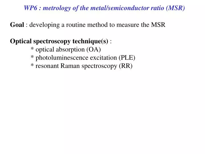
WP6 : metrology of the metal/semiconductor ratio (MSR). Goal : developing a routine method to measure the MSR Optical spectroscopy technique(s) : * optical absorption (OA) * photoluminescence excitation (PLE) * resonant Raman spectroscopy (RR). e -. E 11 fluorescence.

E N D
WP6 : metrology of the metal/semiconductor ratio (MSR) Goal : developing a routine method to measure the MSR Optical spectroscopy technique(s) : * optical absorption (OA) * photoluminescence excitation (PLE) * resonant Raman spectroscopy (RR)
e- E11 fluorescence E22 absorption hole Optical properties : absorption/emission (PL, fluorescence)
e- E11 fluorescence E22 absorption hole Optical properties : absorption/emission (PL, fluorescence) Optical transitions involve excitonic states!
(9,0) (metallic) (10,0) (semi-conducting) (from Saito et al) Electronic and optical properties ‘‘Kataura plot’’ (from Jorio et al)
(9,0) (metallic) (10,0) (semi-conducting) (from Saito et al) Electronic and optical properties ‘‘Kataura plot’’ (from Jorio et al) !! The Eii vary depending on the environment : individual/bundles, gas/liquid matrix, surfactant/substrate… !!
Optical properties : absorption Arc electric sample (1.2 nm<d<1.5 nm) E11,sc E22,sc E11,met (from Izard et al)
E11,sc E22,sc E11,met Optical properties : absorption Arc electric sample (1.2 nm<d<1.5 nm) (from Izard et al)
Optical properties : emission (PL, fluorescence) Only observed on individual semiconducting SWNT (no contacts with metallic) Unbundling Synthesis of individual SWNTs M.J. O’Connell et al., Science 297 (2002) 593 J. Kong et al., Nature 395 (1998) 878 Excitation (661 nm) Emission (850 nm)
Optical properties : NIR fluorescence HiPCO sample (0.7 nm<d<1.3 nm) Identification of a (n,m) nanotube from the couple (Eii,E11) Bachilo et al, Science, 298, 2361 (2002)
Optical properties : Raman scattering E E E 1 1 1 n n n n h ( - ) h ( + ) 0 1 0 1 n n h h 0 0 V = 1 E E E 0 0 0 V = 0 n n h h 1 1 Rayleigh n (h ) Stokes Anti - Stokes 0 n ( ) 1 n ( ) 0 n n n n ( - ) ( + ) 0 cm cm - 1 - 1 0 1 0 1
Optical properties : resonant Raman scattering E E E 1 1 1 n n n n h ( - ) h ( + ) 0 1 0 1 n n h h 0 0 V = 1 E E E 0 0 0 V = 0 n n h h 1 1 Rayleigh n (h ) Stokes Anti - Stokes 0 n ( ) 1 n ( ) 0 n n n n ( - ) ( + ) 0 cm cm - 1 - 1 0 1 0 1
Optical / vibrational properties : (resonant) Raman scattering A1g E2g E1g A1g 1578 cm-1 1583 cm-1 1585 cm-1 200 cm-1 Mode de respiration radial (RBM) Modes d'élongation tangentiels (TM or G-band) Résonance :
Intensité Raman (u.a.) 1400 1500 1600 1700 n -1 (cm ) Resonant Raman scattering E=2.41 eV (l=514.5 nm) Profil semiconducteur Pics symétriques, lorentziens 2.41 eV 1.92 eV E=1.92 eV (l=647.1 nm) Profil métallique Pics assymétriques, couplages électrons-phonons
Resonant Raman scattering Arc electric sample (1.2 nm<d<1.5 nm) nRBM (cm-1) =A/d + B (A≈224, B≈14 cm-1) CVD (HiPCO) sample (0.7 nm<d<1.3 nm) Identification of a (n,m) nanotube from the couple (Eii,nRBM)
WP6 : metrology of the metal/semiconductor ratio (MSR) • Goal : developing a routine method to measure the MSR • Optical spectroscopy technique(s) : absorption, PLE, RR • Method 1 : optical absorption in surfactant-based dispersion • narrowing of the spectroscopic signatures • avoids texture-induced effects • one has to know the OA coefficients • Alternative : measurements on transparent quartz substrates • Method 2 : RR spectroscopy (any substrate) • very high sensitivity and selectivity • one has to mesure the Eii and select a couple of Elaser • one has to measure the RR cross sections (coupling with method 1) • Alternatives : relative (semi-quantitative) measurements • Couplings with PLE and TEM will help!