Download
1 / 3
30 likes | 145 Views
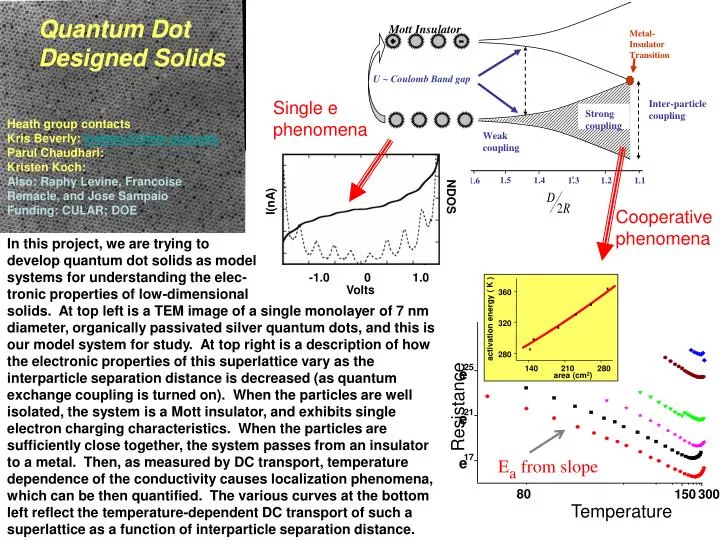
Mott Insulator. Metal-Insulator Transition. 360. U ~ Coulomb Band gap. activation energy ( K ). 320. Inter-particle coupling. NDOS. I(nA). 280. Strong coupling. 140. 210. 280. area (cm 2 ). Weak coupling. 25. e. -1.0. 0. 1.0. Volts. Resistance. 21. e. 1.5. 1.4. 1.3.

E N D
Mott Insulator Metal-Insulator Transition 360 U ~ Coulomb Band gap activation energy ( K ) 320 Inter-particle coupling NDOS I(nA) 280 Strong coupling 140 210 280 area (cm2) Weak coupling 25 e -1.0 0 1.0 Volts Resistance 21 e 1.5 1.4 1.3 1.2 1.1 1.6 17 Ea from slope e 80 150 300 Temperature Quantum Dot Designed Solids Single e phenomena Heath group contacts Kris Beverly: kristen@chem.ucla.edu Parul Chaudhari: Kristen Koch: Also: Raphy Levine, Francoise Remacle, and Jose Sampaio Funding: CULAR; DOE Cooperative phenomena In this project, we are trying to develop quantum dot solids as model systems for understanding the elec- tronic properties of low-dimensional solids. At top left is a TEM image of a single monolayer of 7 nm diameter, organically passivated silver quantum dots, and this is our model system for study. At top right is a description of how the electronic properties of this superlattice vary as the interparticle separation distance is decreased (as quantum exchange coupling is turned on). When the particles are well isolated, the system is a Mott insulator, and exhibits single electron charging characteristics. When the particles are sufficiently close together, the system passes from an insulator to a metal. Then, as measured by DC transport, temperature dependence of the conductivity causes localization phenomena, which can be then quantified. The various curves at the bottom left reflect the temperature-dependent DC transport of such a superlattice as a function of interparticle separation distance.
Heath group contacts: Yi Luo: yiluo@chem.ucla.edu Michael Diehl: diehl@chem.ucla.edu Erica DeIonno: deionno@chem.ucla.edu Greg Ho: gregho@chem.ucla.edu Rob Beckman: beckman@chem.ucla.edu Nick Melosh: nmelosh@chem.ucla.edu Eric Wong: ewwong@chem.ucla.edu Also: Fraser Stoddart Group &Hewlett Packard Corporation Funding: DARPA; SRC; NSF; ONR Molecular Electronics 70 A B SUM Current (10-9 Amps) A 60 B 50 A = 0 0 1 1 B = 0 1 0 1 In this project we are trying to develop molecular electronics-based circuitry for computing applications. This project involves a broad range of scientific challenges, ranging from developing techniques for device scaling to a few nanometers length scale to computer architecture and molecular materials development. Clockwise, from top middle left: An artists version of a molecular switch tunnel junction using [2]catenane molecular switches. The central figure is a distorted micrograph of a 16-bit molecular memory circuit at device size of ~0.0025 microns2. Right top center is data from a 16-bit molecular electronic random access memory circuit; far right is a [2]rotaxane molecular switch. Bottom right is a chemically assembled crossbar circuit using single-walled carbon nanotubes; bottom left is the truth table from an XOR molecular-based logic circuit; middle left is an artists depiction of a molecular electronic nanoscale crossbar.
High throughput proteomics devices 4e-11 Gating Current (Amps) VG = -10 mV VG = 100 mV 2e-11 0 0.00 0.05 0.10 0.15 Time (sec) In this collaboration with the UCLA medical school, and with the School of Engineering, we are trying to develop bio-device platforms for the combinatorial interrogation of transmembrane proteins in highly controlled environments. At top left is a ‘protein’ chip consisting of a lipid bilayer suspended across a pore micromachined into a silicon wafer. Voltage gating of the membrane reveals single channel protein gating characteristics. At top right is our targetted device: a library of cellular membranes in which we utilize fluidics, electronics, sensors, and optics to interrogate the proteins in a host of chemical and physical environments. At bottom left is a picture of a scanning non=linear optical microscope that we have constructed for this project. This microscope utilizes femtosecond laser exciation pulses, and collects the second harmonic generation signal and the two-photon fluorescence signal while retaining full polarization control over both input and output beams. The protein device is scanned in the x,y plane using large amplitude piezeoelectronic scanners. Heath group contacts: Dr. Xin Yang xyang@chem.ucla.edu Dr. Hyeon Choi hchoi@chem.ucla.edu Rigo Pantoja rpantoja@chem.ucla.edu Ryan Riess riess@chem.ucla.edu Also: Francisco Bezanilla (UCLA medical school) & Rich Sayaklly (UC Berkeley) Funding: W.M. Keck Foundation