Download
1 / 12
140 likes | 640 Views
Nanodevices and nanostructures: quantum wires and quantum dots. ECE 423 Final Project Wan-Ching Hung Dec 12,2006. Quantum Dots and Quantum Lines. A quantum dot typically contains between 1 to 200 atoms in diameter and its length, width, and high are generally defined less than 100nm.

E N D
Nanodevices and nanostructures: quantum wires and quantum dots ECE 423 Final Project Wan-Ching Hung Dec 12,2006
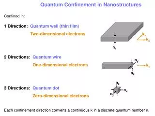
Quantum Dots and Quantum Lines • A quantum dot typically contains between 1 to 200 atoms in diameter and its length, width, and high are generally defined less than 100nm. • The electron is retrained by Fermi wavelength. • Quantum dot is confined in 3 dimensions and quantum line is confined in 2 dimensions.
Quantum Dots Applications • Si single electron transistors • Quantum Computer
Quantum Dots Applications • Nanobarcodes • nanobarcodes are made different quantum wires of different metals that have different reflectivity. • Molecule capsule in drug delivery system
Quantum Confinement • Under 100nm, the wave property of electron can not be ignored.
Coulomb Blockade • a Coulomb blockade is the increased resistance at small bias voltage of an electronic device comprising at lease one low-capacitance tunnel junction.
Self Assembly • Applicatoins: solar cell, light-emitting diodes, capsule in drug delivery system
Lithography and Etching • Lithography: electron beam, ion beam, nanoimprint, dip pen nanolithography • Etching: wet etching, dry etching, plasma, implantation, photo etching
Split-gate Approach • Use additional voltage to create 2 dimensional confinements to control the shape and size of the quantum dot’s gate. • It’s a combination of e beam lithography, evaporation, lift off, contact annealing