Download
1 / 19
190 likes | 314 Views
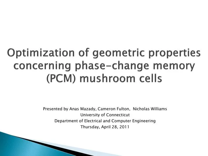
Optimization of geometric properties concerning phase-change memory (PCM) mushroom cells . Presented by Anas Mazady, Cameron Fulton, Nicholas Williams University of Connecticut Department of Electrical and Computer Engineering Thursday, April 28, 2011. Significance. Fast memory

E N D
Optimization of geometric properties concerning phase-change memory (PCM) mushroom cells Presented by Anas Mazady, Cameron Fulton, Nicholas Williams University of Connecticut Department of Electrical and Computer Engineering Thursday, April 28, 2011
Significance • Fast memory • Believed capable of replacing NAND flash • Capable of multi-bit storage • Essential due to low packing density
General Operation • RESET (0) by heating PCM above melting point and quenching • SET (1) by heating PCM above crystallization temperature and below melting temperature • READ by applying very small voltage pulse and measuring current draw (V=IR) • Large current in crystalline phase, smaller current in amorphous phase
Aluminum 100 nm TiN 25 nm NOTE: Geometry is not drawn to scale θ 20 nm GST 7 nm OXIDE 30 nm TiN 5 nm Vpulse Aluminum 40 nm
Materials • Al • High electrical conductivity • Fabrication • SiO2 • Poor thermal conductor • Insulator • TiN • Low thermal conductivity • Adequate electrical conductivity • Heater/heat sink
Phase-change material • Ge2Sb2Te5 (GST) • High crystallization temperature • Low melting point • Adequate Data retention (~10 years at 80°C-90°C)
GST • CMOS compatible fabrication techniques • Minimal thermal crosstalk (65 nm nodes) • Multi-bit storage possible
Variation of theta angle • 0° to 90° • Large active region smaller active region • High peak RESET current lower current • 26% reduction • High peak temperature lower peak temperature • Larger GST area at 90° • Heat diffuses over larger area • Oxide confines heat
Variation of heater contact • 4 nm to 20 nm • Constant theta angle • Constant 1.0 ns voltage pulse • Increase in active region size • Must amorphize entire contact area • Reduction in voltage pulse • Reduction in thermal resistance (oxide) • 10.5 times more RESET current
Aluminum 100 nm TiN 25 nm NOTE: Geometry is not drawn to scale GST 20 nm 7 nm OXIDE 30 nm TiN 5 nm Vpulse Aluminum 40 nm
Specifications • Lateral cross-section: 78.54 nm2 • GST thickness: 20 nm • Erase time: 1.0 ns • Programming voltage: 0.512 V • Read voltage: 150 mV • Low read current: 3.25 nA • High read current:1.04 µA • RESET current density: 133.7 MA/cm2 • Small contact area
Resistance Variation • Low (0) resistance = 46.2 MΩ • High (1) resistance = 144.2 kΩ • ~320 times less resistance • 2-3 orders of magnitude • Large range • Multi-bit storage
READ operation IPEAK = 3.25 nA R = 46.2 MΩ IPEAK = 1.04 µA R = 144.2 kΩ