Download
1 / 26
270 likes | 499 Views
Phase change memory technology Rob Wolters. September 2008. Contents. Introduction Phase change materials Memory cell concepts Switching Endurance Retention Perspective. Control gate. Floating gate. SiO 2. Si 3 N 4. Polysilicon. Programming and erasing the floating gate.

E N D
Phase change memory technologyRob Wolters September 2008
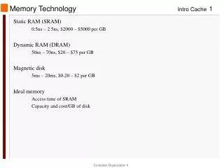
Contents • Introduction • Phase change materials • Memory cell concepts • Switching • Endurance • Retention • Perspective
Control gate Floating gate SiO2 Si3N4 Polysilicon Programming and erasing the floating gate Control gate High voltage “Thick” gate oxide Double poly Floating gate
performance is stagnating! forever! density is improving! for how long? Introduction (present NVM)
‘225’ Sb-M SbTe-M SEM picture of DVD-RW dots Phase change materials
DVD-RW materials on chip What is the PC RAM challenge: How to integrate into
PE word-lines • PE based on a switching resistance • Phase-change materials amorphous phase: ‘high’-Ohmic • crystalline phase: ‘low’-Ohmic • Fast switching between amorphous and crystalline phase bit-lines PC RAM principle • A simple scalable device: • An access transistor and a programmable element (PE) • High switching speed (~ns) • Read/write endurance: >1012 (Flash: 106) • Memory array with NMOS transistors:
Small amorphous volume ~20 nm3 ! Phase change technology: Ovonyx cell(Ovshinsky in 1966) Ovonyx cell 1T – 1R cell Sidewall spacer contact
NXP Approach: Novel cell concept & Material “NXP novel line concept” (top view) Small area highest resistance = Electrode material = Phase-change material Cell concepts • Megabit demonstrators by Intel, STM, Samsung Ovonyx concept “Ovonyx concept” (cross section) Small volume undergoes phase change Small contact area between PC-layer and electrode
Metal contacts (TiN) line of phase-change material Thickness: 15 nm Width: 50nm Length: 1000 nm Line concept
Switching Electric pulses induce Joule heating RESET pulse: - T > Tmelt - Rapid cooling down amorphization SET pulse: - T > Tcryst - Longer pulse crystallization
PE word-lines bit-lines Phase-change materialsCell switching RESET Electric pulses induce Joule heating RESET pulse: - T > Tmelt - Rapid cooling down amorphization P = I2 . R (Joule heating) I: determined by technology node For optimum energy transfer: RPE = Rtransistor (~2 k Ω) RPE = ρ . L/A
Phase-change materialsCell switching RESET 20 nm 5 nm Ireset as a function of line width for 20 and 5 nm thick PC, L=2W
Phase-change materialsCell switching SET Amorphous state shows a threshold voltage
1.4 PE 1.2 word-lines 1 Amorphous 0.8 Idut [mA] 0.6 Crystalline 0.4 0.2 Threshold voltage 0 -0.5 0 0.5 1 1.5 2 2.5 Vdut [V] bit-lines Cell switching Vdut = VT . L V: determined by technology node VT : material characteristic V = 1-2 V, L < 100 nm
Phase change cell Passivation TaN Electrode Metal 2 Via & Trench Metal1 W-plugs STI STI STI Process integration PC cells embedded in a standard CMOS process Top view SEM Cross-section SEM
Integrated Test Cells SET RESET Sensing window in SET/RESET resistance2 kb memory sub-sector
Imin+15% Endurance
Retention DVD: amorphous dots in a crystalline matrix Size: appr. 300 x 300 nm PC cell: amorphous dot and crystalline areas aside. Size: appr. 50 x 100 nm System tends to the lowest energy: crystallinity!
Retention DVD: amorphous dots in a crystalline matrix Increased doping Ga15Sb75
Positioning of amorphous spot. Thomson Effect • Thermoelectric effect • IEDM 2007
Perspective • PCM performance • Fast (~50 ns) • Low voltage (0.4-2 V) • Scaling: good • Medium endurance (109-1013) • Medium current (50-300 A) • Energy (pJ/switch) • PCM costs • Only 3 additional masks • NVM/Flash performance • Slow (s-ms) • High voltage (10-15 V) • Scaling: bad • Short endurance (105-106) • Low current (~ nA) • Energy (nJ/switch) • NVM/Flash costs • 8-10 additional masks