Download
1 / 32
380 likes | 759 Views
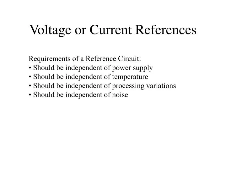
Voltage or Current References. Requirements of a Reference Circuit: Should be independent of power supply Should be independent of temperature Should be independent of processing variations Should be independent of noise. S = ( D V ref / V ref ) / ( D V dd / V dd ).

E N D
Voltage or Current References • Requirements of a Reference Circuit: • Should be independent of power supply • Should be independent of temperature • Should be independent of processing variations • Should be independent of noise
S = ( D Vref / Vref ) / ( D Vdd / Vdd ) Vref Vdd Voltage or Current References • Requirements of a Reference Circuit: • Should be independent of power supply • Should be independent of temperature • Should be independent of processing variations • Should be independent of noise Sensitivity:
S = ( D Vref / Vref ) / ( D Vdd / Vdd ) Vref Vdd Voltage or Current References • Requirements of a Reference Circuit: • Should be independent of power supply • Should be independent of temperature • Should be independent of processing variations • Should be independent of noise Sensitivity: If sensitivity = 1, then 10% change in Vdd results in a 10% in Vref
Simple Bias Circuits Vdd Vout GND Typically using a potentiometer
Vref S = 1 Vdd Simple Bias Circuits Vdd Vout GND Typically using a potentiometer
Vdd Vout GND Vref S = 1 Vdd Simple Bias Circuits Vdd Transistor-based resistive divider Vout GND Typically using a potentiometer
Vdd Vout GND If KN = KP and VTN = |VTP| Vref Vref S = 1 S = 1 Vdd Vdd Simple Bias Circuits Vdd Transistor-based resistive divider Vout GND Typically using a potentiometer
Vdd Vout GND If KN = KP and VTN = |VTP| Vref Vref S = 1 S = 1 Vdd Vdd Simple Bias Circuits Vdd Transistor-based resistive divider Vout GND Typically using a potentiometer Typically poor Power Supply Rejection (low PSRR)
Iout GND Current Source Bias Circuits involving Diodes MOSFET Source Vdd R Vout GND
BJT Source Vdd Iout R Vout GND Current Source GND Bias Circuits involving Diodes MOSFET Source Vdd R Vout GND
BJT Source Vdd Iout R Vout GND Current Source GND Bias Circuits involving Diodes MOSFET Source Vdd R Vout GND Significant Power Supply Rejection (higher PSRR)
Output Voltage Sensitivity Small-Signal model: BJT Source Vdd Vdd R R Vref Vref 1/gm GND GND
Output Voltage Sensitivity Small-Signal model: BJT Source Vdd Vdd Vref = Vdd / (1 + gm R) R R gm = (Vdd0 – Vref0)/ RUT Vref Vref 1/gm GND GND
Vref S = (Vref / Vdd) (Vdd0 / Vref0) = (Vdd0/Vref0)/(1 + (Vdd0–Vref0)/UT) Vdd Output Voltage Sensitivity Small-Signal model: BJT Source Vdd Vdd Vref = Vdd / (1 + gm R) R R gm = (Vdd0 – Vref0)/ RUT Vref Vref Vref(1 + (Vdd0 – Vref0)/ UT) = Vdd 1/gm GND GND
Vref S = (Vref / Vdd) (Vdd0 / Vref0) = (Vdd0/Vref0)/(1 + (Vdd0–Vref0)/UT) Vdd Output Voltage Sensitivity BJT Source Vdd R Vref GND
Vref Vref S = (Vref / Vdd) (Vdd0 / Vref0) = (Vdd0/Vref0)/(1 + (Vdd0–Vref0)/UT) S = (Vdd0/ (Vdd0–Vref0)) (UT / Vref0) Vdd Vdd Output Voltage Sensitivity BJT Source Vdd R Vdd0–Vref0 >> UT Vref GND
Vref Vref S = (Vref / Vdd) (Vdd0 / Vref0) = (Vdd0/Vref0)/(1 + (Vdd0–Vref0)/UT) S = (Vdd0/ (Vdd0–Vref0)) (UT / Vref0) Vdd Vdd Output Voltage Sensitivity BJT Source Vdd R Vdd0–Vref0 >> UT Vref ~1 GND
Vref Vref Vref S = (Vref / Vdd) (Vdd0 / Vref0) = (Vdd0/Vref0)/(1 + (Vdd0–Vref0)/UT) S = (Vdd0/ (Vdd0–Vref0)) (UT / Vref0) S = 0.04 Vdd Vdd Vdd Output Voltage Sensitivity BJT Source Vdd R Vdd0–Vref0 >> UT Vref ~1 GND With Vref0 ~ 0.65,
Allows wider variation of output voltage Bias Circuits involving Diodes Vdd R Vout R1 GND R2 GND Significant Power Supply Rejection (high PSRR)
Breakdown Diode Reference Big Issue: Very noisy output voltage
Bootstrapped Reference Vdd Vdd M4 M3 AI = (W/L)1 / (W/L)2 Vout2 Iref Vout1 M1 M2 GND R GND
V Bootstrapped Reference Vdd Vdd M4 M3 AI = (W/L)1 / (W/L)2 Vout2 Iref Vout1 M1 M2 GND R GND
V Bootstrapped Reference Vdd Vdd M4 M3 AI = (W/L)1 / (W/L)2 Vout2 In subthreshold (or BJTs): V = UT ln(AI) = Iref R Iref = UT ln(AI) / R Iref Vout1 M1 M2 GND R GND
Iref Iref V GND Bootstrapped Reference Vdd Vdd Vdd M4 M3 AI = (W/L)1 / (W/L)2 Vout2 In subthreshold (or BJTs): V = UT ln(AI) = Iref R Iref = UT ln(AI) / R Iref Vout1 M1 M2 GND R GND
Startup Circuit Bootstrapped Reference
Startup Circuit Bootstrapped Reference