Download
1 / 30
310 likes | 477 Views
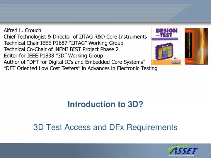
Alfred L. Crouch Chief Technologist & Director of IJTAG R&D Core Instruments Technical Chair IEEE P1687 “IJTAG” Working Group Technical Co-Chair of iNEMI BIST Project Phase 2 Editor for IEEE P1838 “3D” Working Group Author of “DFT for Digital IC’s and Embedded Core Systems ”

E N D
Alfred L. Crouch Chief Technologist & Director of IJTAG R&D Core Instruments Technical Chair IEEE P1687 “IJTAG” Working Group Technical Co-Chair of iNEMI BIST Project Phase 2 Editor for IEEE P1838 “3D” Working Group Author of “DFT for Digital IC’s and Embedded Core Systems” “DFT Oriented Low Cost Testers” in Advances in Electronic Testing Introduction to 3D? 3D Test Access and DFx Requirements
The Truth about Moore’s Law So, who suffers? Fab Tool Providers… …they only have 5customers left…
The 3D Business: Why 3D? • Okay, Moore’s Law – transistors get tinier, die get bigger, wafers get bigger, microprocessors make more money…yadda, yadda, yadda • Fabs are starting 28nm production right now • It might, maybe, could, we think…be cheaper to stack die on top of each other instead of shooting for going below 7nm • …and how do you keep making Fabs when there are fewer of them every year (the Fab parts supplier gets below critical customer mass)… • What else may be driving this? • Form-Factor – How small can we make an iPhone? How much memory do you want in a thumb drive? Can we get a 10M-pixel camera in our sunglass frames? HDTV in our glasses? • Performance – It may be better to stack optimized die like Processors in a great logic process and Memory in an ideal memory proccess and to put them close together (Vertical is 30u – Horizontal could be 200u)
The 3 Main 3D Business Paradigms • The main one today is Homogenous Die Stacking • Memory growth by stacking identical memory die • One thought is to reorganize a chip – like a microprocessor and to distribute it in 3-Dimensions • Smaller Die size, things closer together • Owned by one design group/company/organization • TSV’s put in with layout tools too meet local layout goals • The other idea is to create a “competitive socket” and to have “die-providers” vie for the space (the hard one) • Open like a hard-core business • Source and Second-Source • Yield-Management • Standards Based (not just Test, but features, locations) • Drill & Fill or manufactured as Upper-Die
The 3D Die Types • A Base/Bottom Die will be similar to die today • Will have board/socket connections • Will have bumps on top to pass on connections • Must pass Powers & Grounds up to “the Stack” • Base connection may be an interposer • All other die will be “Middle or Upper Die” • Only bumps on both sides (or only on bottom for Top Die) • Minimal or no probe pads (no ESD protection either) • It may be possible to define a “Top Die” (i.e. RF emitter, no top bumps) • Providing a die to be used as both a Base and an Upper will probably be two (or more) different design efforts • Stacking order depends on market and possibly some engineering considerations (power, number of TSV’s, heat-generation…) • e.g. bottom die is a processor, next is the memory, then die is stacked by the amount of power & grounds needed; or by thermal considerations
The 3D Description and Problem • We’ve been making Stacked-Things for quite a while • SIPs, PoPs, FLIPs, FLOPs… • Did we learn anything usable from this? • Testing was still individual chips then packaging (bond wires, glue, velcro, duct tape…) • What is different about what we call 3D • Through-Silicon-Via’s (TSV’s) make direct buried die-to-die connections • Bare die have no pins (maybe no Pads) • Manufacturing of TSV’s is potentially destructive • Wafer-Thinning and Back grinding • Laser drilling and metal filling • TSV’s are similar to today’s Via’s • Voids, inconsistent filling (there is no such thing as a good via…) • The smaller the via and closer the via pitch, the more problems with resistance, inductance and capacitance • No disassembly when a die is found to be bad…
3D – The Stack FPGAProgrammable Die Interposer Upper Die Upper Die Interposer Base Die
3D Drill & Fill doesn’t buy back area 1:1 Direct probing may result inpotential damageNote: no ESD protection Bump Pitch • Via Size + Keep-Out Zone • Via Pitch / Bump Pitch • Logic Spreading to accommodate TSVs • e.g. 300K TSV’s consume 1mm^2 Bump Size Via Size No logic/routes in this area Via Pitch
Comparison of TSV to On-Chip Interconnect http://www.monolithic3d.com/tsv-vs-monolithic-3d.html Remember 2um = 2000nm Compared to 28nm objects (a) Illustration of TSV in a 3D-IC, and (b) ITRS Projections
“TSV” by Makoto Motoyoshi http://emlab.uiuc.edu/tsv/Yokohama_paper.pdf A SEM image of 60x60 um^2 TSVs after deep Si etch
3D TSV’s in microns, Bumps limiting factor STATS ChipPAC also offers a 300mm post-TSV “mid-end” fabrication process flow that occurs between the wafer fabrication and back-end assembly process. Mid-end processes support the advanced manufacturing requirements of 2.5D and 3D TSV, as well as wafer-level packaging, flip chip and embedded die technology.The mid-end process includes temporary bonding/de-bonding, back-side via reveal, silicon recess and back-side metallization and microbumping. Microbump is required to meet fine pitch, low profile applications in 3D TSV, stacking and assembly. STATS ChipPAC offers 60/40um pitch microbump bonding.
3D In the News http://www.electroiq.com/articles/ap/2011/06/3d-ic-prototyping.html3D IC prototyping process result of MENT, Tezzaron, MOSIS collaborationJune 16, 2011 -- Mentor Graphics Corporation (NASDAQ:MENT), in a cooperative effort with Tezzaron Semiconductor and MOSIS, created a process for economically developing and manufacturing 3D-IC prototypes on multi-project wafers (MPWs). The process enables designs using tens of millions of through silicon vias (TSVs) with dimensions as small as 1.2 x 6µm and 2.4µm pitch, producing up to 300,000 vertical interconnects per mm2.MOSIS's Multi Project Wafer (MPW) services now allow users, via Tezzaron, to test out 3D-IC concepts using the same provider and model they currently use for their standard semiconductors, said Wes Hansford, director at MOSIS, who added that resource and schedule coordination reduces the "effort and risk" in moving silicon roadmaps forward. MOSIS manages MPW projects including reticle creation, fab reservations, final packaging and testing, and other logistics.Tezzaron enhances customer designs as required for successful 3D-IC integration and also provides backend manufacturing steps including wafer thinning, backside metal and wafer bonding.Mentor Graphics provides DRC and LVS tools that support 3D-IC physical verification, ensuring that designs are correct and will meet 3D process requirements. Mentor Graphics brings production-certified Calibre solutions to the prototyping step, verifying that "3D-IC designs are manufacturable," said Joseph Sawicki, VP and GM of the Design-to-Silicon Division at Mentor Graphics. "The Calibre solution uses foundry-certified PDKs from MOSIS wafer suppliers with extensions for MOSIS-Tezzaron 3D-IC designs."Customers can use the 3D-IC service to create proof-of-concept ICs that demonstrate the use of high-density TSVs in stacked die configurations for intelligent sensor, multi-core processor and many other applications. MOSIS is a low-cost prototyping and small-volume production service for VLSI circuit development. For more information about the 3D-IC prototyping service, visit www.mosis.com.Tezzaron Semiconductor specializes in 3D wafer stacking, TSV processes, and cutting-edge memory products. Learn more at www.tezzaron.comMentor Graphics Corporation (NASDAQ:MENT) provides electronic hardware and software design solutions. Learn more at http://www.mentor.com/.
Cascade Microtech: Replaceable Contact Layer http://atevision.tttc-events.org/Best_ATE_Paper_Award/KGD_Probing.ppt • Tips are 5 um square and 20 um tall • 35 um pitch array • 24 x 48 tips
Cascade Microtech: Probe marks on ENIG TSV pad http://atevision.tttc-events.org/Best_ATE_Paper_Award/KGD_Probing.ppt • Exaggerated conditions: 10 TDs at 2.5 gf • Navigation grid (50 x 40 um) shows 3 probe marks on the 100 um diameter pad
Today’s 3D vs Future 3D • Flat Layout • Units take up N-S/E-W space • Routing distance is N-S/E-W lengths • Stacking is displacement for TSV andsimilar on top of base • Mostly today’s CAD/CAE Tools • Vertical Layout from the start • Core/Elevators at heart of design • Routing distance is X, Y, or Z lengths • Stacking is engineering consideration(thermal, route-distance, RF, noise, etc.) • New CAD/CAE Tools
What is the Big Picture in the Chip World? • Embedded Content has grown with Moore’s Law • Cores include embedded content that becomes doubly or triply embedded logic (IEEE 1500 was created to assist with test access and portability) • Test Logic is no longer just used at Wafer-Probe or ATE IC Test • Fault Tolerance and reliability demands embedded runtime features • Standardized Access to embedded content (Instruments) that is available at Wafer, IC, Board, and System is needed Mem-Core CPU Core Mem-Core DSP Core Mem-ConfigASIC Mem-ConfigASIC AnalogCore Mem-Core Mem Core VoltageMonitor LBIST MBIST MBIST MBIST Scan & LBIST Scan & LBIST BIST MBIST Scan &Debug Scan &Debug Mem-Core Mem-Core CPU Core PowerConfig PowerConfig ASICCore FLASHCore RF Core FLASHCore ProcessMonitor MBIST MBIST Process Monitor Process Monitor Scan MBIST MBIST RF-BIST • Die Stacking has added a level of complexity to accessing embedded content (how is a Core’s LBIST on the 2nd die in a stack accessed and operated?) • These chips are showing up onboards with board/system test requirements • IEEE P1687 and P1149.7 were both started to address these issues SerDes Mem-Core Mem-Core GlueLogic PowerConfig EmbeddedRepair EmbeddedRepair Mem-Core Mem-Core Mem-Core Tuning & Programing MBIST & DMA MBIST MBIST Scan Temp Monitor Temp Monitor Temp Monitor MBIST MBIST TAP Controller Base Die Die #2 Die #3 JTAG
What’s the Problem – Upper Die? Access to Embedded Test & DebugIssue Die-Test Isolation Issue DSP Core Mem Core CPU Core CPU Core Scan &Debug Scan &Debug LBIST MBIST Scan & Debug Expensive die & Yield Multiplier Issue Probe Pad forWafer Test orStack Issue 1500 Wrapper 1500 Wrapper 1149.1 TAP & Ctrl ASIC Core HOTSpot TempMon Security & Trust Issue Number of Vias&Wherefor Test Issue Scan Die ID New Defect Models Issue FLASH Core Existing Standard Issue 1149.1 TAP & Ctrl Chip-to-ChipInterconnectTest Issue MBIST 1149/1500 Boundary Scan What Test Features Issue Upper Die
Going Forward to 3 Dimensions • 2D Chip Test Issues still exist • DFM still requires a lot of work • Requires more complex vectors than just stuck-at • Favors moving DFx logic onto the chip • DFx is helpful to the Board/System developer • Cores create the first level “access” problem • High-Speed I/O requires tuning • 3D Die Stacking aggravates the situation • It becomes a multiplied “access” problem • It creates concerns over temperature hot spots • It creates concerns with noise immunity • Test-scheduling, Test-Cost, Test-Interference • More opportunities for Security and Trust issues
What are we Testing? Chip vs Board 3D Test is acombination of Both • There are Chip (IC) Tests • Fault Coverage (e.g. Stuck-At, Path Delay, Transition Delay, n-Detect) • Defect Coverage (shorts, opens, bridges, GOS) • Parametrics (Max FRQ, Leakage – iDDQ, IOH,IIL, VOH, VIL) • Functional (Read, Write, Bus Transactions, etc.) • Embedded BIST (Logic, Memory, HSIO) • There are Board Tests • PCOLA • SOQ • FAMI
What’s Addressing the Issues? • Is anybody brave enough to take on all of these issues – based on two industries: • Chip and Board • …across several environments • Wafer Probe, Bare-Die Test, Stacked-Die Test • Board Test, Board Characterization, System Test • …with new issues • Thermal concerns • Massive Interconnect • Yield Multiplication
P1838 – Par Approved: Thanks Erik Jan Marinissen First Name 1. Saman 2. Lorena 3. Patrick Y 4. Paolo 5. Sandeep 6. Vivek 7. Eric 8. Adam 9. Al 10. Shinichi 11. Ted 12. Bill 13. Jan Olaf 14. Michelangelo 15. Said 16. Michael 17. Gert 18. Hongshin 19. Rohit 20. Santosh J 21. Philippe 22. Stephane 23. Hans 24. Erik Jan 25. Teresa 26. Ken 27. Herb 28. Mike 29. Andrew 30. Daniel 31. Jochen 32. Volker 33. Eric 34. Thomas 35. Ioannis 36. Min-Jer 37. Lee Last Name Adham Anghel Au Bernardi Bhatia Chickermane Cormack Cron Crouch Domae Eaton Eklow Gaudestad Grosso Hamdioui Higgins Jervan Jun Kapur Kulkarni Lebourg Lecomte Manhaeve Marinissen McLaurin Parker Reiter Ricchetti Richardson Rishavy Rivoir Schöber Strid Thaerigen Voyiatzis Wang Whetsel Affiliation TSMC IMAG-TIMA IBM Politecnico di Torino Atrenta Cadence Design Systems DfT-Solutions Synopsys Asset-Intertech Panasonic Cisco Cisco Neocera Politecnico di Torino Delft University of Technology Analog Devices TTU Cisco Synopsys Synopsys ST Microelectronics ST-Ericsson Qstar Test IMEC ARM Agilent Technologies eda2asic/GSA AMD Univ. of Lancaster TEL Verigy edacentrum Cascade Microtech SussMicroTec TEI of Athens TSMC Texas Instruments Job Title Senior Manager Design Technology Assistant Professor Product Director Senior Architect, DFT Synthesis and Verification Man. Director and Principal Trainer and Consultant Principal Engineer Chief Technologist, Director of IJTAG R&D Panasonic resident at imec Staff Engineer Distinguished Manufacturing Engineer Global Sales and Applications Manager Post-doc researcher Senior Test Development Engineer Senior research fellow Technical Leader Senior R&D Engineer DfT senior engineer SoC DFT & Test Specialist CEO Principal Scientist DFT Manager and Technical Lead Senior Scientist President DFT Architect Professor Product Marketing Manager System Architect Head of EDA Cluster Research Chief Technical Officer Bus. Man. FA Products and 3D Integration Test Professor Test Development Manager Distinguished Member Technical Staff Location Canada Grenoble, France UK Torino, Italy San Jose, California, USA Endicott, New York, USA Fareham Hampshire, UK Allentown, Pennsylvania, USA Austin, Texas, USA Leuven, Belgium San Jose, California, USA San Jose, California, USA San Francisco, California, USA Torino, Italy Delft, the Netherlands Limerick, Ireland Tallinn, Estonia San Jose, California, USA Mountain View, California, USA India Grenoble, France Grenoble, France Brugge, Belgium Leuven, Belgium Austin, Texas, USA Loveland, Colorado, USA California, USA Boxboro, Massachusetts, USA Lancaster, UK Austin, Texas, USA Boeblingen, Germany Hannover, Germany Beaverton, Oregon, USA Dresden, Germany Athens, Greece Hsinchu, Taiwan Dallas, Texas, USA The Study Group that led to the PAR Chair: Erik Jan Marinissen (IMEC) Vice-Chair: Adam Cron (Synopsys) Secretary: Sophocles Metsis (AMD) Editor (US): Al Crouch (ASSET) Editor (EU): Michael Wahl (U. Siegen) Currently: 42 active members And many more over the past few weeks!
The P1838 3D Test Working Group Goal • 5.2 Scope of Proposed Standard: The proposed standard is a ‘die-centric’ standard; it applies to a die that is pre-destined to be part of a multi-die stack and such a die can be compliant (or not compliant) to the standard. The proposed standard defines die-level features, that, when compliant dies are brought together in a stack, comprise a stack-level architecture that enables transportation of control and data signals for the test of (1) intra-die circuitry and (2) inter-die interconnects in both (a) pre-stacking and (b) post-stacking situations, the latter for both partial and complete stacks, in both pre-packaging and post-packaging situations. The primary focus of inter-die interconnect technologies addressed by this standard is Through-Silicon Vias (TSVs); however, this does not preclude its use with other interconnect technologies such as wire-bonding. • The standard will consist of two related items. • 1. 3D Test Wrapper On-die hardware features that enable transportation of test (control and data) signals in the following configurations. • • Pre-stacking: From on-die I/Os to die-internal DfT features, and vice versa. • • Post-stacking • ‘Turn’ mode: From on-die I/Os to die-internal DfT features, and vice versa. These on-die I/Os might be external I/Os and/or inter-die interconnections coming from (or going to) an adjacent die. • ‘Elevator’ mode: From on-die I/Os, through THIS DIE, to the inter-die interconnections to an adjacent die, and vice versa. These on-die I/Os might be external I/Os and/or inter-die interconnections coming from (or going to) another adjacent die. • 2. Description A description of the Test Wrapper features in a standardized human- and computer-readable language. This description should allow the usage of the die within a multi-die stack for test and test access purposes. To investigate whether an IEEE Standard is needed to cover 3D chips – the consensus was YES! This includes Physical, Architecture, and Descriptions
Current Status • Just finished defining the “per-die” requirements • Must have an access mechanism • Must be able to be tested in a standalone manner • Must support 4 access functions (Bypass, Turnaround, On-Die, and Next-Die) • Next step is to define the “per-stack” requirements • Must test the connectivity of TSV’s between Die • Must verify the die in the stack (e.g. Die-ID’s) • Must verify the order of dies in the stack • Must verify the number of die in the stack
Will IEEE Standards be involved? • 1149.1 is the Base Standard that provides the “protocol” • Instruction-Based • Register-Based • Defines the “State-Machine” • Defined to assist with Board Test • Described with BSDL/SVF • 1500 is a derivation used for Core Test • Instruction-Based • Register-Based • Defined to assist with Cores (Virtual Chips) • Described with CTL/STIL • 1687 is a departure to address certain weaknesses in 1149.1/1500 • Vectors are defined for the Instrument • Mixes Instruction and Data • Network-Based (variable length scan paths) • Described with ICL/PDL • 1149.7 can reduce 1149.1’s TAP to just 2 Pins • Defines a TDMA packet protocol
3D P1687 SIB Access Architecture TDI TDO TCK Select ShiftEn CaptEn UpdEn RST Top Interface of Die Turn-Around orNext-Die Access TDIb TDIa WSIb WSIa Ua Ub Sb Sa TDOb TDOa Select-b Select-a WSOa ab 00 = turnaround (2-bit) 01 = next-die (2-bit bypass) 10 = on-die access only 11 = on-die + next-die access WSOb On-Die Access Bottom Interface of Die TDI TDO TCK Select ShiftEn CaptEn UpdEn RST
The 1500 3D-WIR TDI SWIR TDO TCK Select ShiftEn CaptEn UpdEn RST Next-Die Access Up No TDI-TDO Strap Needed on Down Instructions Next (1) 0 Instructions: Up = Next, Byp, WBR-Upper,On-Die-Shared, SWIR Down = Turnaround,WBR-Lower, On-Die-Only Byp (1) WBR-Upper WBR-Lower On-Die (n) Turnaround (1) WSO W I R Turn-Around WSI SWIR Down TDI SWIR TDO TCK Select ShiftEn CaptEn UpdEn RST
The 1149.1 3D TAP No TDI-TDO Strap Needed on Down Instructions Next-Die Access TDI TMS TCK TDO Up Up Next (1) 1 Instructions: Up = Next (On-Die-Shared), Bypass, WBR-Upper, Down = Turnaround,WBR-Lower, On-Die-Only Byp (1) WBR-Upper WBR-Lower On-Die (n) Turnaround (1) Do all TAPS need to be 100% Synch’edor can a Synch Process (RTI) be used? TDI TDO IR TAPSM Turn-Around Down TDI TMS TCK TDO
The Multi-Access-Mechanism – Mixed Access Up Instructions &Down Instructions Upper Die with 1500 Upper Die with 1687 SiBa EIB SiBb Up Instructions &Down Instructions Next (1) Next (1) Byp (1) Byp (1) TAPSM WBR-Upper WBR-Upper WBR-Lower WBR-Lower On-Die (n) On-Die (n) Base Die with TAP Turnaround (1) Turnaround (1) IR IR TDI TDI TDI TDI TCK TCK TCK TCK TDO TDO TDO TDO TMS TMS TMS TMS Select Select Select ShiftEn ShiftEn ShiftEn CaptEn CaptEn CaptEn UpdEn UpdEn UpdEn RST RST RST SelectWIR SelectWIR SelectWIR Board Pin Connections
Will 3D Silicon Integration become real? No ConclusionYou Decide! acrouch@ASSET-InterTech.com