Download
1 / 34
350 likes | 896 Views
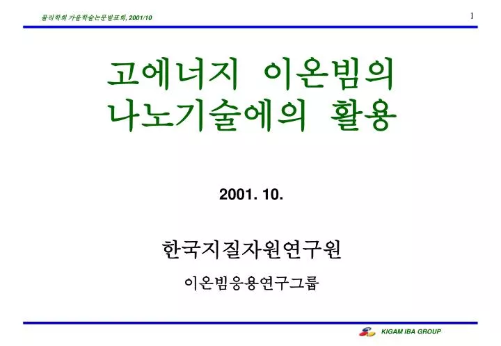
고에너지 이온빔의 나노기술에의 활용 2001. 10. 한국지질자원연구원 이온빔응용연구그룹. Contents High energy ion beam engineering Micro-engineering P-lithography & LIGA technology Waveguide & microlens fabrication 3-D micro-machining using micro-beam Micro-actuator (electrostatic comb drive) Nano-engineering

E N D
고에너지 이온빔의 나노기술에의 활용2001. 10.한국지질자원연구원이온빔응용연구그룹
Contents • High energy ion beam engineering • Micro-engineering • P-lithography & LIGA technology • Waveguide & microlens fabrication • 3-D micro-machining using micro-beam • Micro-actuator (electrostatic comb drive) • Nano-engineering • Ion Projection Lithography (IPL) • Smart cut technology • Magnetic nanostructure patterning • Nanocrystal synthesis & optoelectronic application
Interaction of MeV Ions with Matter • large number of low E transfer collisions with electrons & small number of large E transfer collisions with nuclei • approximate straight line motion with small angle scattering in the sample • relatively high range (47.8 mm in Si for 2 MeV Proton) • small degree of straggling (1.0 mm range straggling in Si for 2 MeV Proton) • analytical point of view • non-destructive & absolute • insensitive to charging effect & depth profiling possible
Micro & Nano-engineering using Ion Beams • LIGA Technology • Advantages of the LIGA Technology • large range of materials: metals, alloys, plastics, ceramics • variety of designs possible • structures over 1 mm high • high precision into the sub mm range • low cost mass production Proton LIGA Technology
초소형 기어 및 격자 시험 제작 • Photomask 제조 • e-beam writing • 5” photo-mask 제조 • 이온빔 마스크 제조 • PR형성 및 UV 조사 • Au 전기도금 • Si 후면 건식식각 • PR 에칭 • 미세구조물 제작 • PMMA층 형성 • 양성자조사 (2.4 MeV, 4x10¹³/cm2) • PMMA식각 및 Ni도금 • PMMA 및 Ti희생층 제거 Overall Ion Beam LIGA Process
Ion Implantation Chamber 4” Ion Beam Mask Micro-structures of Small Gear and Honey-comb Array
Polymeric waveguide제조 및 특성조사 • 이온빔 조사에 의한 PMMA의 특성변화 Refractive index depth profile in planar waveguide, (350 keV H+ 6×10¹⁴ ions/cm2 ) • 매입형(buried) waveguide 구조형성 • 응용분야 : 광스위치, 광 분기회로, 간섭계 등 • H+ implantation : 1.8 MeV, 5×10¹³ ions/cm2주입 • 광특성조사 : nano-fiber시스템 이용 Mask patterns (5x2.5mm2) for waveguide and lithography. From the top, straight waveguide, Y-branch waveguide, Mach-Zehnder interferometer
매입형 waveguide 광특성 Microscope images of the photomask fabricated for ion mask. Side-view of buried planar waveguide in PMMA formed by 1.8 MeV proton implantation. End-view of Y-branch waveguide in PMMA formed by 1 MeV H+ implantation. • 무기 waveguide (LiNbO3, KNbO3, BaTiO3등) 형성 • 유기고분자 단점 (내열성, 광학손실) 극복 • 우수한 전자광학, 음향광학, 비선형 광특성 보유 및 희토류 doping 용이성 • 기존 방법으로는 waveguide 형성이 가능한 결정소재가 제한됨 • 이온주입법에 의한 waveguide (Er: Ti[Zn]: LiNbO3) 제조 • He 이온주입 : optical index barrier 형성 • Er 이온주입 : 1.54 mm 광방출, active waveguide 형성, 일체형 집적 광학소자 제조
마이크로빔을 이용한 3D 가공기술 • 매질내 양성자 비정이 명확히 정의되는 특성을 이용 • 양성자 LIGA기술에 바탕을 둠 • 직경 20-100 mm의 반구(hemi-sphere) 및 임의의 패턴 형성 Basic Steps of the Techniques for Producing Microstructures with Curved Surfaces
마이크로 렌즈 제조기술 • 차세대 광통신/광컴퓨터의 핵심부품인 고분자 마이크로렌즈/ 어레이 제작 Optical Components in Optical Information System Fabrication Process of Micro-lens Array
Micro-actuator 제작 • 구동방식 : 정전형 comb-drive • 일차구조재 : Ni • 사양 • 크기 : 2600x1100 mm2 • 두께 : 40 mm • 정전기력 : 26 mN at 60V • 변위 : 5 mm • 공명주파수 : 1780 Hz Layout of Electrostatic Micro-resonator
Nano-technology Au 4 nm Au 30 nm Nano-gear Carbon nanotubes Artist’s impression of scanning probe lithography Striking colors arise from gold nanocrystals formed in sapphire and fused silica by ion implantation. Encapsulated gold nanocrystals produce purple or red. (ORNL)
반도체공정용 이온빔 리소그라피 • Ion Projection Lithography Ion Projection Lithography System & Proton Exposure Result
Smart Cut Technology • Why SOI? • for VLSI dedicated to low-voltage (<1 V), low-power, high-speed systems • for Gb DRAM generation and the system on chip approach • other market segments : • radiation-hard circuits, smart power, MEMS • mixed signal, high temperature electronics, integrated optics • SOI market • currently $40 million/yr • annual growth rate : 40 - 50 % • projected to reach 10 % of the Si market by the year 2005 • smart cut • more cost-effective & better quality than conventional BESOI (Bonded & Etch back SOI) process • 300 mm SOI wafers available
Patterned exfoliation using ion implantation • geometric patterning of substrate using ion implantation induced exfoliation • an alternative approach to that of multi-step, selective etching in III-V heterostructures in optoelectronic devices • target substrate : InP, GaAs, InGaAsP/InP • experimental • ion implantation : 450 keV H (4x10¹⁶ ions/cm2), 1 MeV He (1x10¹⁷ ions/cm2), • annealing : 350 ºC -400ºC for a few min. with ramp rate of 100ºC/s SEM image of InP(100) containing a buried InGaAsP layer implanted with 1.0 MeV He ions. The implant mask consisted of Au stripes, 2 mm thick and 8 mm wide. SEM image of GaAs(100) implanted with 450 keV protons. The sidewall along the (110) plane is very vertical and smooth.
Magnetic nanostructure patterning • 기존방법 • 전자빔 패터닝, stamping & replication, holography 식각 • resist공정이므로 디스크세정이 문제됨 • 이온빔 주입법 • 비접촉식 패터닝 : Si stencil 마스크나 초집속이온빔(FIB) 사용 • 자기다층 : Co/Pt (10-14 periods of 4 Å Co & 10 Å Pt) • 이온주입 : 1016 ions/cm2 of 700 keV N+ • 이온 mixing에 의한 자기층 교란 및 자기비등방성 상실 • FIB Patterning : ultimate pitch of ~50 nm expected (256 Gbits/in2) Kerr hysteresis data; (a) the polar Kerr loop for the as deposited film. (b) the polar Kerr loop for the irradiated area, and (c) the longitudinal kerr loop for the irradiated area. (a) Schematic of ion beam irradiation through a Si stencil mask. (b) SEM image of Si mask. (c) MFM(magnetic Force Microscope) image showing magnetic contrast. (IBM)
Nano-particulate Technology • 나노입자 제조기술 • 기계적 방법 • 고에너지 볼밀링 (air-jet, 습식) • 물리적 방법 • 스퍼터링 • 증발법 • 화학적 방법 • inert gas condensation (IGC) • chemical vapor condensation (CVC) • microwave plasma process (MPP) • low pressure combustion flame process (LPCFP) • 액상합성 • 이온주입법 • nanocystal (nanocluster) 제조
Nanocrystal synthesis • nanocrystal의 특성 • 전기적, 광학적, 자기적, 열역학적 특성이 급변함 • 결정크기에 따른 발광파장 변조 (Mie scattering) • 양자점(quantum dot)의 단전자 터널링 • 일반 제조방법 • 습식화학합성 • RF sputtering, laser ablation • MBE (Molecular Beam Epitaxy) • 이온주입법 • 주입원자의 과포화 및 고온 열처리 석출법 • 공정의 다양성 : 실용화에 대비한 최적 방법중 하나임 • 주요 예상 용도 • 광소자 : 광스위치, 광기억소자, waveguide 등 • 단전자 소자 : SET (Single Electron Transistor), tera-bit memory, 양자컴퓨터 등 quantum quantum quantum well wire dot 물질의 차원에 따른 전자들의 상태밀도(자유도) 변화 : 전자 및 에너지 양자화 양자점에 소스, 드레인, 게이트 세 단자가 연결된 SET 회로의 개략도
Nanocrystal synthesis with ion implantation • 이온주입법 • high dose(1016-1017 ions/cm2) 이온주입에 의한 주입원자의 과포화 • 고온 열처리(Ar + 4% H2)에 의한 주입이온 석출 및 나노결정 형성 (5-30 nm) • 각종 금속 및 반도체 (Si, Ge, SiGe, GaAs, GaP, GaN, InAs,, InP, CdS, CdSe, CdSeS, CdTe, CdSeTe, ZnS, ZnSe, PbS 등) 나노결정 생성가능 • 주요 매질 : Si, SiO2, sapphire(Al2O3) 등 • 이온주입방법의 특징 • non-equilibrium technology : 주 매질, 주입이온과 무관한 다양한 조합가능, 과포화형성 용이 • 2개 이상의 phase 혼재가능 : 복합물질 NC 형성가능 • 밀도, 크기, 깊이제어 용이 • 주 매질 내부에 위치하므로 내구성 유지 • 기존 VLSI, ULSI 공정과 호환가능 • 문제점 : 입도의 불균일성, 이온주입에 따른 방사선상해, 경계면에 대한 이해부족
Nanocrystal Si-based optoelectronic devices • Si의 광소자 소재로서의 문제점 • indirect bandgap에 의한 발광의 비효율성 • 선형 전자광학효과의 부재로 인한 변조의 비효율성 • 따라서 전자소자(Si)-광소자 통합을 위한 신개념의 광전자소자 개발이 요구됨. • Si 발광 연구 • Si내 희토류원소 doping 또는 Si NC 형성 • 집적 광전자소자 (광스위치, 광도파관, 발광-수광 소자) 개발 • Si NC 광전자 소자 • Si NC의 tunable bandgap : 1.4~2.2 eV (1.1 eV for bulk crystal) • NCs 광전자소자 제조공정 : Si 반도체공정과 100% 호환 • Si NC 제조방법 • deposition onto substrates by gas phase synthesis • PECVD(Plasma Enhanced CVD) : decomposition of silane (SiH4) by plasma • Si ion implantation
Enhanced rare earth luminescence in Si NCs • Er doping of Si • 1.54 mm 발광 : 광통신용 광섬유 전달계수가 극대화됨 • 상온에서는 비방사전이에 의해 발광효율은 실용화수준에 못 미침 • Er doped Si NC • quantum confinement와 Er doping 기술의 결합 • Si NC : 공명에너지 전달체(sensitizer) 역할 • 상온에서 고효율 발광특성 실현 • Si NC : 공명에너지 전달체(sensitizer) • Er은 SiO2내 존재하므로 Si 매질에서의 비방사전이가 억제됨 • Experimental • Si NC 형성 : 이온주입, PECVD (2-4 nm crystals in 300 nm silica substrate) • Er 주입 및 PL 특성조사 (488 nm laser)
Er doped Si NC의 PL특성 Room temp. PL spectra for SiO2 and Si NC samples implanted with Er ions. Room temp. PL spectra of Er-implanted Si NCs at different Er doses. Temperature dependence of the PL signal at 1.54 mm.
Ferromagnetic nanoparticles • 장래의 초고밀도 자기자료저장수단 : 기존의 1만배 • single-particle-per-bit • discrete, magnetically isolated, single domain ferromagnetic nanoparticles • 이온주입법 활용가능 • Fe, Ni, Co NCs in YSZ(Yttrium-stabilized Zirconia) or sapphire • NCs들이 공간적으로 서로 잘 분리되며, 결정 정렬과 자기특성 제어 가능 • 실용화까지는 NC 위치제어 등 다수의 난제들이 남아 있음 Magnetic hysteresis results and corresponding micro-structure for Co NCs in sapphire. Crystallographically oriented “nanocubes” of a-Fe embedded in YSZ.
There is plenty of room at the nano-world for ion engineering. You have a free choice!