Download
1 / 20
200 likes | 207 Views
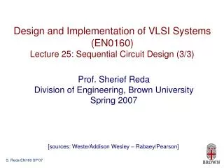
Design and Implementation of VLSI Systems (EN0160) Lecture 22: Material Review. Prof. Sherief Reda Division of Engineering, Brown University Spring 2007. [sources: Weste/Addison Wesley – Rabaey/Pearson]. dope with phosphorous or arsenic n-type. dope with boron p-type.

E N D
Design and Implementation of VLSI Systems (EN0160) Lecture 22: Material Review Prof. Sherief Reda Division of Engineering, Brown University Spring 2007 [sources: Weste/Addison Wesley – Rabaey/Pearson]
dope with phosphorous or arsenic n-type dope with boron p-type Impact of doping on silicon resistivity silicon 4.9951022 atoms in cm3 Resistivity 3.2 105 Ωcm 1 atom in billion 88.6 Ωcm 1 atom in million 0.114 Ωcm 1 atom in thousand 0.00174 Ωcm 1 atom in billion 266.14 Ωcm 1 atom in million 0.344 Ωcm 1 atom in thousand 0.00233 Ωcm Electrons are more mobile/faster than holes
A Al p n B One-dimensional representation Use P and N material to make diodes and transistors and gates
IC manufacturing Spin resist Expose (using mask) Develop resist ACTION (e.g., implant) Remove Resist
NMOS transistor, 0.25um, Ld = 10um, W/L = 1.5, VDD = 2.5V, VT = 0.4V The MOS transistor has three regions of operation • Cut off Vgs < Vt • Linear (resistor): Vgs > Vt & Vds < Vgs-Vt Current α Vds • Saturation: Vgs > Vt and Vds ≥ Vgs-Vt Current is independent of Vds
Non-ideal Shockley vs actual operation • Channel length modulation: • Increasing Vds • decreases channel length • increases current Velocity saturation: At high electric field, drift velocity rolls off due to carrier scattering Temperature dependency
desired regions of operation V in V out CMOS inverter noise margins
Use equivalent circuits for MOS transistors Ideal switch + capacitance and ON resistance Unit nMOS has resistance R, capacitance C Unit pMOS has resistance 2R, capacitance C Capacitance proportional to width Resistance inversely proportional to width Simple RC delay models
ON transistors look like resistors Pullup or pulldown network modeled as RC ladder Elmore delay of RC ladder Elmore delay model
Logical effort to calculate gate delay • g: logical effort= ratio between input capacitance of the gate to that of an inverter than would deliver the same current • h: electric effort = ratio between load capacitance and the gate input capacitance (sometimes called fanout) • p: parasitic delay • represents delay of gate driving no load • set by internal parasitic capacitance
Logical effort generalizes to multistage networks Path Logical Effort Path Electrical Effort Branching factor Path Effort F=GBH Effort of Multistage logic networks
Optimization using logical effort models Delay of multi-stage network is minimized when each stage bears the same effort Optimal number of stages
Dynamic Short circuit power (dynamic) Static (leakage) Power Techniques to reduce power: clock gating, multiple Vdd, multiple Vt, temperature,
Interconnects They have resistance and capacitance → contribute to delay and dynamic power Distributed vs lumped Elmore delay model How to calculate delay (gate + wires)?
Interconnects Coupling capacitance introduces cross talk which depends on the switching activity of the neighboring wires. Cross talk increases delay and causes noise • Solutions to interconnect problems • 1. Width, Spacing, Layer • 2. Shielding • 3. Repeater insertion • 4. Wire staggering and differential signaling • 5. Buffer insertion (what are the locations/optimal number?) • 6. Staggering and differential signaling
Implications of ideal device scaling devices interconnects
Logic families • Asymmetric gates (favors one input) • Skewed gates (favors one transition) • How to calculate logical effort? Families to get rid of some of static CMOS problems: help in one way, introduces another problem domino CPTL Pseudo-NMOS (ratioed circuits) PTL Cascode Voltage Switch Level
Circuit Design Pitfalls variations Design in corners make sure you have enough margins