Download
1 / 34
350 likes | 500 Views
Electron-phonon interactions in a SWCNT-DNA hybrid nanostructure. Alfredo D. Bobadilla Nanotechnology course – Prof Jorge M. Seminario Spring 2010 Texas A&M University. Table of Contents. INTRODUCTION MOTIVATION OBJECTIVE BASIC CONCEPTS REVIEW OF PREVIOUS WORKS

E N D
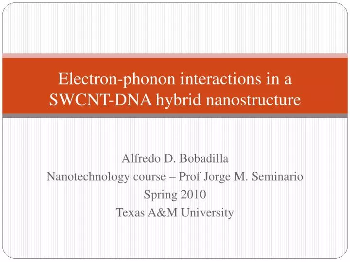
Electron-phonon interactions in a SWCNT-DNA hybrid nanostructure Alfredo D. Bobadilla Nanotechnology course – Prof Jorge M. Seminario Spring 2010 Texas A&M University
Table of Contents • INTRODUCTION • MOTIVATION • OBJECTIVE • BASIC CONCEPTS • REVIEW OF PREVIOUS WORKS • RESEARCH PROJECT PROPOSAL • CONCLUSIONS • REFERENCES
INTRODUCTION • Nanotechnology has focused for a long time on the synthesis of nanomaterials. • Nowadays there is enough knowledge about physical and chemical properties of some nanomaterials to be able to put them to work together. • Carbon nanotubes own the highest electrical conductivity and the highest mechanical stiffness. • DNA own unique self-assembly properties which enable a precise design of DNA-based molecular networks.
MOTIVATION • Optical spectroscopy methods are not adequate for characterization of nanoelectronic sensors and devices, they were developed for studying bulk material properties. • Novel methods are required to characterize a single molecule or few molecules nanosystem. • DNA and CNT own unique physical and chemical properties which make them ideal elements for a broad range of engineering applications.
OBJECTIVE • Detecting vibrational modes in a suspended CNT-DNA hybrid nanostructure, necessary requirement to ensure the nanodevice was properly assembled. SWCNT diameter ~1.5nm, DNA diameter ~1.8nm Au electrodes Si wafer
Basic concepts: Scattering theory • Scattering is a process where moving particles are forced to deviate from a straight trajectory by one or more localized non-uniformities in the medium through which they pass. • Elastic scattering is a type of scattering in which the kinetic energy of the incident particles is conserved, only their direction of propagation is modified. • In inelastic scattering the kinetic energy of an incident particle is not conserved. In this scattering process, the energy of the incident particle is lost or gained. • When an electron is the incident particle, the probability of inelastic scattering, depending on the energy of the incident electron, is usually smaller than that of elastic scattering. http://en.wikipedia.org/wiki/Inelastic_scattering
Basic concepts: Quantum tunnelling • Tunneling is the quantum mechanical process by which a particle can penetrate a classically forbidden region of space (for example, passing from two separate points A and B without passing through intermediate points). The phenomenon is so named because the particle, in traveling from A to B, creates a sort of "tunnel" for itself, bypassing the usual route. http://scienceworld.wolfram.com/physics/Tunneling.html
Basic concepts: Quantum tunnelling Schematic representation of quantum tunnelling through a barrier. The energy of the tunneled particle is the same, only the quantum amplitude (and hence the probability of the process) is decreased. The scale on which these "tunnelling-like phenomena" occur depends on the wavelength of the traveling wave. For electrons, the thickness of "the tunnelling barrier" is typically a few nanometres. http://en.wikipedia.org/wiki/Quantum_tunnelling
Basic concepts: STM (Scanning tunneling microscope) • A STM is a powerful instrument for imaging surfaces at the atomic level. • It is based on the concept of quantum tunneling. When a conducting tip is brought very near to the surface to be examined, an applied voltage can allow electrons to tunnel through the vacuum between them. http://en.wikipedia.org/wiki/Scanning_tunneling_microscope
Basic concepts: Inelastic Electron Tunneling Spectroscopy (IETS) • IETS is an experimental tool for obtaining the vibrational spectra by detecting changes in a tunneling current due to inelastic scattering process. • In a tunneling current electrons experience elastic scattering, but if the applied bias voltage is high enough some electrons will experience inelastic scattering, exciting vibrations in the molecule and observing a small change in the current. • The small change in the current is clearly noticeable in the second derivative. http://en.wikipedia.org/wiki/Inelastic_electron_tunneling_spectroscopy
Basic concepts: Inelastic Electron Tunneling Spectroscopy (IETS) • Experimentally, the first and second derivative of the I –V curve is obtained by a lock-in amplifier technique. • The voltage applied across the tunnel junction is an AC small signal Vω superimposed onto a DC bias signal VG. The current through the junction can be written as a Taylor expansion. C. Petita and G. Salace, Rev. Sci. Instrum. (2003)
Basic concepts: Lock-in amplifier • Lock-in amplifiers are used to detect and measure very small AC signals (pico and nanovolts). Accurate measurements may be made even when the small signal is obscured by noise sources many thousands of times larger. • They achieve this by acting as a narrow bandpass filter which removes much of the unwanted noise while allowing through the signal which is to be measured. Noisy signal http://www.boselec.com/products/siglimwhat.shtml
Review of previous works:STM-based molecular junctions • An STM is used to form a molecular junction aiming to measure the conductivity of an N-alkanedithiol molecule. • The gold-Nitrogen affinity make it possible the formation of a covalent bond between N-alkanedithiol molecules and each metal gold electrode. • Alkanedithiol molecules are in solution on a gold substrate. http://www.zurich.ibm.com/~bmi/REVFIG4.JPG
Review of previous works:STM-based molecular junctions • Initially the STM gold tip is approached until making contact with the gold substrate, and when slowly retracted it is formed a gold wire of a few atoms. • When the gold nanowire is present it’s detected quantized values of conductance which decrease (as the tip is moved out) until a minimum value before the gold nanowire breaks. B Xu and NJ Tao, Science (2003)
Review of previous works:STM-based molecular junctions • The STM tip continues being retracted and at a critical point the gold nanowirebreaks. • When the gold nanowirebreaks it’s still detected quantized values of conductance but much lower than before. • Those conductance values are attributed to the N-alkanedithiol molecules. B Xu and NJ Tao, Science (2003)
Review of previous works:STM-based molecular junctions • After the molecular junction is formed, it continues to be separated by pulling out the STM tip until another molecule configuration occurs and the first and second derivative is again recorded. • The phonon spectrum for the molecular junction changes with changes in contact geometry or molecular configuration due to stretching conditions. A STM allows conductance measurements and a Lock-in amplifier allows measuring first an second derivative of the I-V curve at each molecular configuration. Hihath et al, NanoLett. (2008)
Review of previous works:STM-based molecular junctions • Figure (a) is the histogram of conductance, it shows how many times was found each measured value of conductance. • The big peak correspond to the gold wire and the small one corresponds to the N-alkanedithiol molecule. • Figure (b) shows how measured conductance values change as the molecule is stretched. Hihath et al, NanoLett. (2008)
Review of previous works:STM-based molecular junctions • Figures (c) and (d) show how the vibrational spectra changes at different stretching conditions. Hihath et al, NanoLett. (2008)
Review of previous works:microfabricatedmolecular junctions • Single-molecule conductance and IET spectra are measured on benzenedithiolate connected to gold electrodes to identify the number and type of organic molecules within metal–molecule–metal junctions. M. Taniguchi, IOP nanotechnology (2009)
Review of previous works:microfabricated molecular junctions • An electromechanical system allow a precise control on the molecule stretching. • The piezo-driven pushing element cause a bending of the substrate on which it is supported the molecular junction. M. Taniguchi, IOP nanotechnology (2009)
Review of previous works:microfabricated molecular junctions • Quantized values of conductance are detected for different molecule stretching conditions. M. Taniguchi, IOP nanotechnology (2009)
Review of previous works:microfabricated molecular junctions • Vibrationalspectra changes at different stretching conditions. • The selection rule for IET spectra agrees with that for Raman spectroscopy. • Asymmetrical differential conductance suggests asymmetrical electrode–molecule coupling. M. Taniguchi, IOP nanotechnology (2009)
Review of previous works: A DNA duplex bridging a CNT gap • A 10nm gap is created in a single-walled CNT. • CNT is functionalized with carboxyl groups and DNA with amine groups. • A peptide bond is formed between CNT and DNA by a dehydration reaction. • After the reaction, the DNA bridge the CNT gap. Current is different than zero after connecting with DNA the CNT gap. Guo et al, Nature nanotechnology (2008).
Review of previous works: CNT electromechanical model • A doubly clamped suspended CNT is deflected by an electrostatic force generated by the applied voltage between gate and nanotube. • The heavily n doped Si substrate acts as a back gate. • In this geometry, van der Waals forces can be neglected. Lefevre et al, Physical Review Letters (2005).
Review of previous works: CNT electromechanical model • An AFM allow measuring the maximum deflection as a function of the applied gate voltage. • The CNT deflection only depends on its physical properties and on the electrostatic environment given by the connecting and gate electrodes Lefevre et al, Physical Review Letters (2005).
Review of previous works: CNT electromechanical model • A continuum model is developed which is valid for CNTs of different diameters D and lengths L. • ‘y’ variable represent CNT deflection. • The model allows determining the maximum deflection uMAX of the CNT as a function of an electrostatic force controlled by a gate voltage (VG). Lefevre et al, Physical Review Letters (2005).
Research project proposal: general description • V1 DCand V2 DC allow controlling CNT deflection and therefore DNA stretching. • By using IETS, vibrational modes are detected for different stretching conditions. SWCNT diameter ~1.5nm, DNA diameter ~1.8nm Au electrodes Si wafer V1 DC V2 DC
Research project proposal : general description Initial state (VG=0) After applying gate voltage (VG≠0)
Research project proposal: CNT positioning by dielectrophoresis • A CNT suspension (with acetone as solvent) is prepared and a drop of it is deposited between electrodes while a composite electric field is being applied between electrodes to orient and position an individual suspended CNT.
Research proposal: microfabricationprocess and DNA connection
Conclusions • A novel method has been proposed to perform a DNA stretching experiment. • The generation of tension in the hybrid nanostructure and the measurement of its vibrational modes are both made by electrical means. • The proper characterization of this hybrid nanodevice allow testing its integrity and correct assembly. • One important application of this nanodevice is on detection of chemical and biochemical events at the single molecule level.
References Science 29 August 2003, Vol. 301. no. 5637, pp. 1221 - 1223 Measurement of Single-Molecule Resistance by Repeated Formation of Molecular Junctions http://www.sciencemag.org/cgi/content/abstract/301/5637/1221 NanoLett., 2008, 8 (6), pp 1673–1678 Study of Electron−Phonon Interactions in a Single Molecule Covalently Connected to Two Electrodes http://pubs.acs.org/doi/abs/10.1021/nl080580e Masateru Taniguchi et al 2009 Nanotechnology 20 434008 Inelastic electron tunneling spectroscopy of single-molecule junctions using a mechanically controllable break junction http://iopscience.iop.org/0957-4484/20/43/434008;jsessionid=D D3A3BDF6F14111A0C02519250ACEEDA.c2
References Rev. Sci. Instrum. 74, 4462 (2003); doi:10.1063/1.1611995 Inelastic electron tunneling spectrometer to characterize metal–oxide– semiconductor devices with ultrathin oxides http://rsi.aip.org/rsinak/v74/i10/p4462_s1?isAuthorized=no Nature Nanotechnology 3, 163 - 167 (2008) Conductivity of a single DNA duplex bridging a carbon nanotube gap http://www.nature.com/nnano/journal/v3/n3/abs/nnano.2008.4.html Phys. Rev. Lett. 95, 185504 (2005) Scaling Law in Carbon Nanotube Electromechanical Devices http://prl.aps.org/abstract/PRL/v95/i18/e185504